Oxidation in microtechnology refers most often to the oxidation of silicon. A layer of silicon dioxide created on the surface of a silicon wafer can be easily patterned.
An SiO2 layer can be created by thermal oxidation or by deposition.
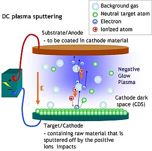
Energetic ions sputter material off the target which diffuse through the plasma towards the substrate where it is deposited. There is no strong plasma glow around the cathode since it takes a certain distance for the plasma to be generated by electron avalanches started by a few secondary electrons from the sputtering process.
Y. Okinaka, in Electroless Plating: Fundamentals and Applications, edited by Glenn O. Mallory and Juan B. Hajdu, Chapter 15, American Electroplaters and Surface Finishers Society (1990).
Photo and electron beam resists as well as many other polymers are often coated on wafers by spinning a volatile solution of the compound onto the wafer.