Analogue Electronics/pn Junctions
This page quickly recapitulates the concepts of a pn junction, and its basic behaviour. For a more detailed analysis, see the Semiconductors Wikibook and the Materials in Electronics Wikibook.
Electron States and Doping
[edit | edit source]Electrons in a solid lattice must exist in certain electron states. Due to interaction between the atoms in the lattice, these states are grouped into energy bands, separated by energy gaps, in which no states exist. Therefore electrons cannot exist in these energy gaps.

In a semiconductor, at absolute zero (0K) bands up to and including the valence band are completely full of electrons. The conduction band - the next band above the energy gap above the valence band (called the band gap)- is completely devoid of electrons. The same goes for all bands higher than the conduction band.

Electrons in bands which are either completely full or completely empty cannot contribute towards a current, so a semiconductor at 0K is a perfect insulator. At higher temperatures, thermal energy causes some electrons to jump the band gap and exist in the conduction band. These electrons, along with the holes that were left when the electron departed the conduction band can now contribute to carrying a current. As the temperature rises, more and more electrons can make this jump and the semiconductor becomes more conductive.
Semiconductors can have impurities added to introduce more electrons or holes to make p-type or n-type semiconductors. These conduct predominantly with one kind of carrier:
| n-Type Material | p-Type Material |
The pn Junction
[edit | edit source]When a p-type semiconductor is joined to an n-type semiconductor, the interface between the two is called a pn junction.
Because the electron concentration in the n-type material is much higher than in the p-type material, electrons will tend to diffuse across the junction into the p-type material. Likewise, holes will tend to diffuse from the p-type to the n-type material.
Since the materials had, on their own, no net charge, this diffusion sets up a charge imbalance. The n-type material, which has lost electrons and gained holes now has a net positive charge, and the p-type material, which has lost holes and gained electrons, has a net negative charge. This creates a potential difference between the two types of material, which will act against the diffusion of holes and electrons, pulling them back to where they started. This opposing flow of charge under a potential difference is called drift.

At equilibrium, these two effects will balance out, and no net current will flow:
- Hole diffusion from p-type to n-type equals hole drift from n-type to p-type
- Electron diffusion from n-type to p-type equals electron drift from p-type to n-type
A region near the junction will have no charge carriers present, as they have recombined with their counterparts from the other type of material. This area is called the depletion zone, or sometime the space-charge region. Charged particles still exist here, but they are the nuclei of the atoms in the lattice, and cannot move.
At equilibrium, a potential still exists between the two materials and it is referred to as the built-in voltage or potential barrier. An electric field, is set up across the depletion zone by the presence of the unbalanced charges left in the depletion zone by the departure of the charge carriers. In the depletion zone's n-type material side, the atoms left have a net positive charge (they are missing one electron), and on the p-type side, they have a net negative charge, due to the extra electron acquired.
The electric field therefore is directed from the n-type material to the p-type material:

As shown in this figure, the remaining electrons in the n-type material have to overcome the potential barrier (and move against the electric field) in order to move across the junction (from right to left), and similarly, the holes need to overcome it to move from left to right. Remember that there are very few free holes in the n-type material, and very few electrons in the p-type material, so no current can possibly flow this way.
In order to overcome the potential barrier, an external potential can be applied across the junction.
Biased pn Junctions
[edit | edit source]The first thing to note when considering the action of an external electric field is that the semiconductor that is outside the depletion region is highly conductive compared to the depletion region. This means that any potential difference applied to the device will be concentrated across the depletion region, and will not manifest itself as an electric field in the un-depleted semiconductor.
Forward Biased Junction
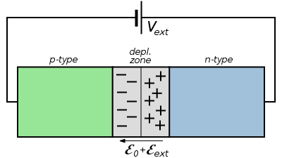
[edit | edit source]Imagine connecting the pn junction to a voltage source so that the n-type material is at a lower potential than the p-type. The electric field from the external potential difference, , acts against the internal electric field, . This gives a total electric field of :

This means that the electric field opposing the flow of charge carriers is also reduced, and so some carriers will diffuse across. The reduced electric field will bring the junction to equilibrium again, but the depletion zone will be shorter. The band diagram for this situation is shown below:

The reduced potential barrier also means the some electrons and holes with thermal energy can "jump" across the depletion zone, whereupon they will be swept out of the semiconductor by the applied voltage. If the external potential is greater than the internal potential, the barrier is reversed, and electrons and holes can flow virtually unimpeded through the junction - once the barrier voltage is exceeded, a very large current can flow.
Reverse-Biased pn Junction
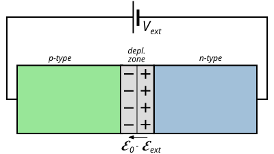
[edit | edit source]Now, consider connecting the junction so the n-type material is at a higher potential than the p-type material. The electric field induced by the external potential will reinforce the internal potential and make it :

This will force more charge carriers out of the area around the junction, making the depletion zone larger. The increased potential barrier means that charge carriers need more energy to jump the depletion zone, and the external field is acting against them anyway:

This means that no current due to majority carriers (electrons in the n-type and holes in the p-type) will flow across the junction.
The only current that can possibly flow in this situation is a tiny leakage current, composed of minority carriers (holes in the n-type material and electrons in the p-type). As these are very sparse, this current is very small (usually only a few nanoamps).
IV Characteristics of a pn Junction
[edit | edit source]Careful consideration of the above effects leads, as demonstrated in Semiconductors, to the following equation describing the pn junction:
[Ebers-Moll Equation]
where
- IS is the reverse saturation current (caused by thermal activity - generally on the order of 20nA for "normal" voltages)
- VT is the thermal voltage (about 25mV at room temperature)
- V is the applied voltage
- I is the current across the junction
This is called the "Ebers-Moll" model of a pn junction.
A diode following this model exactly has very extreme characteristics - the current becomes huge after the potential barrier is exceeded, and is tiny in reverse bias. The plot below exaggerates the reverse current and lessens the growth of the forward current for clarity.

When V is not very close to 0, we can approximate, to a good degree of accuracy, the current as follow:
For forward bias,
For reverse bias,
Generally, the value of V0 is taken to be about 0.7V. This is when the junction begins to provide extremely little resistance to the current flowing. Even though current flows before this value, it is small (much smaller than shown on the diagram).
Further reading
[edit | edit source]- Materials in Electronics Wikibook, for a description of the energy bands in semiconductors.
- Semiconductors Wikibooks, for a more detailed analysis of the pn junction.


