File:CMOS AND Layout.svg
Jump to navigation
Jump to search

Size of this PNG preview of this SVG file: 375 × 250 pixels. Other resolutions: 320 × 213 pixels | 640 × 427 pixels | 1,024 × 683 pixels | 1,280 × 853 pixels | 2,560 × 1,707 pixels.
Original file (SVG file, nominally 375 × 250 pixels, file size: 21 KB)
|
|
This is a file from the Wikimedia Commons |
Summary
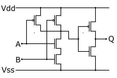
| Description | Layout of NMOS and PMOS components in a 2-Input AND gate |
| Date | 12/07/06 |
| Source | Own drawing, Inkscape 0.43 |
| Author | inductiveload |
| SVG development |
Licensing
| I, the copyright holder of this work, release this work into the public domain. This applies worldwide. In some countries this may not be legally possible; if so: I grant anyone the right to use this work for any purpose, without any conditions, unless such conditions are required by law. |
File history
Click on a date/time to view the file as it appeared at that time.
| Date/Time | Thumbnail | Dimensions | User | Comment | |
|---|---|---|---|---|---|
| current | 19:20, 24 March 2014 | | 375 × 250 (21 KB) | Wereldburger758 | Valid SVG now. |
| 19:02, 12 July 2006 |  | 375 × 250 (29 KB) | Inductiveload | {{Information |Description=Layout of NMOS and PMOS components in a 2-Input AND gate |Source=Own drawing, Inkscape 0.43 |Date=12/07/06 |Author=inductiveload |Permission=PD |other_versions= }} Category:CMOS |
File usage
The following 3 pages use this file:
Global file usage
The following other wikis use this file:
- Usage on de.wikibooks.org
- Usage on fr.wikibooks.org
- Usage on fr.wikiversity.org