Super NES Programming/Super FX tutorial
Introduction[edit | edit source]
The SuperFX is a custom 16-bit RISC processor with a special bitmap emulation function designed for the Super NES. It was designed to bring rudimentary 3D capabilities to the SNES. Programming for it is done with special Super FX assembly language. Each SuperFX title uses a combination of standard SNES assembly code with specially compiled SuperFX assembly routines coded as binary data in the cartridge. It can run in parallel with the SNES under certain conditions. Each SuperFX cartridge has on-board RAM which the SuperFX chip uses as a frame buffer and for general purpose operations which it can share with the Super NES.
Existing titles[edit | edit source]
The SuperFX chip was used in 8 released SNES games, in Star Fox 2 (unreleased) and in multiple tech demos; 2 of which binaries are available.
| Title | SuperFX Version | ROM Size | Work RAM Size | Save RAM Size |
|---|---|---|---|---|
| Starfox/Starwing | Mario Chip | 8 MBit | 256 KBit | None |
| Dirt Racer | GSU-1 | 4 MBit | 256 KBit | None |
| Dirt Trax FX | GSU-1 | 4 MBit | 512 KBit | None |
| Stunt Race FX | GSU-1 | 8 MBit | 512 KBit | 64KBit |
| Starfox 2 | GSU-1 | 8 MBit | 512 KBit | 64KBit |
| Vortex | GSU-1 | 4 MBit | 256 KBit | None |
| Voxel(demo) | GSU-1 | 3 MBit | 512 KBit | None |
| Powerslide(demo) | GSU-1 | 3 MBit | 512 KBit | None |
| DOOM | GSU-2 | 16 MBit | 512 KBit | None |
| Yoshi's Island | GSU-2-SP1 | 16 MBit | 256 KBit | 64KBit |
| Winter Gold | GSU-2 | 16 MBit | 512 KBit | 64KBit |
Theory of Operation[edit | edit source]

The SuperFX is a co-processor for the SNES CPU. The SuperFX's task is to execute complex mathematical calculations much faster than the SNES and to generate bitmap pictures for simple 3D rendering of SuperFX games. The SuperFX and SNES processors share access to a common Work RAM and Game pak ROM bus. Only one of the SuperFX or SNES CPU may access the game pak ROM and RAM at any time, controlled by special registers. The flow of the SNES and SuperFX accessing the data busses is an art in optimizing the program's efficiency.
The RAM inside the SuperFX cart is different from battery backup RAM - it can be used for storing results of calculations, for storing a SuperFX program, for storing bulk data or for storing a PLOT picture the SuperFX is generating. There is 256 Kib (32KiB) or 512 Kib (64 KiB) of RAM.
The SuperFX can process instructions in 3 ways: reading them from game pak RAM, from the gamepak ROM (reading straight out of the ROM chip), or via a special 512 byte instruction cache.
It is possible for the SuperFX to run in parallel with the SNES CPU when using the 512 byte instruction Cache. It involves loading a program in, and then setting the SuperFX to start its work. The 512 byte cache is in general 3x faster compared to running the program in the game pak RAM or ROM. The SuperFX can interrupt the SNES CPU after it finishes processing.
When using the special bitmap functions of the SuperFX it's possible to quickly load the bitmap out of the gamepak into the SNES Video RAM and display it on the screen. The SNES by default is a tile and sprite based console - pixel based scene construction used in 3D rendered games is very inefficient with stock SNES hardware. In SuperFX games such as DOOM, Starfox/Starwing and the like, the SuperFX is rapidly painting pixel based scene bitmaps onto the game pak RAM and then throwing it into the SNES VRAM for graphics display many times per second.
Hardware revisions[edit | edit source]
There are 3 different hardware revisions of the SuperFX. All revisions are functionally compatible in terms of instruction set but support different ROM sizes.
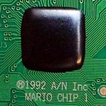
- MARIO Chip - which stands for Mathematical Argonaut Rotation Input Output. The first release of the SuperFX chip and was only used with Starfox/Starwing. There are two versions of the chip - one with a direct PCB die bonded/epoxied setup and one with a standard chip carrier package.
- GSU-1 - the release used on most SuperFX games in a standard chip carrier package. Functionally identical to MARIO Chip. Supports maximum 8Mbit (1 Megabyte) ROM size.
- GSU-2 - used on the final 3 SuperFX games, supports the full 16 Megabit (2 Megabyte) ROM size.
-
 MARIO chip (Packaged)
 -
 MARIO chip (Epoxied)
 -
 GSU-1
GSU-1 -
 GSU-2
GSU-2 -
 GSU-2 SP1


Registers[edit | edit source]
The SuperFX registers are mapped from $3000-$32FF. Some are 16-bit; some are 8-bit. The explanation of each register is shown in this section. $3100-$32FF is the Instruction Cache.
Overview[edit | edit source]
The Super FX chip has 16 general-purpose 16-bit registers labeled R0 to R15 plus 11 control registers. Additionally, a memory space from $3100-$32FF forms the instruction cache
| Register | Address | Description | Access from SNES |
R0 |
$3000 |
default source/destination register | R/W |
R1 |
$3002 |
pixel plot X position register | R/W |
R2 |
$3004 |
pixel plot Y position register | R/W |
R3 |
$3006 |
for general use | R/W |
R4 |
$3008 |
lower 16 bit result of lmult | R/W |
R5 |
$300A |
for general use | R/W |
R6 |
$300C |
multiplier for fmult and lmult | R/W |
R7 |
$300E |
fixed point texel X position for merge | R/W |
R8 |
$3010 |
fixed point texel Y position for merge | R/W |
R9 |
$3012 |
for general use | R/W |
R10 |
$3014 |
for general use | R/W |
R11 |
$3016 |
return address set by link | R/W |
R12 |
$3018 |
loop counter | R/W |
R13 |
$301A |
loop point address | R/W |
R14 |
$301C |
rom address for GETB, GETBH, GETBL, GETBS |
R/W |
R15 |
$301E |
program counter | R/W |
Control Registers
| Name | Address | Description | Size | Access from SNES |
SFR |
$3030 |
status flag register | 16 bits | R/W |
$3032 |
unused | |||
BRAMR |
$3033 |
Backup RAM register | 8 bits | W |
PBR |
$3034 |
program bank register | 8 bits | R/W |
$3035 |
unused | |||
ROMBR |
$3036 |
rom bank register | 8 bits | R |
CFGR |
$3037 |
control flags register | 8 bits | W |
SCBR |
$3038 |
screen base register | 8 bits | W |
CLSR |
$3039 |
clock speed register | 8 bits | W |
SCMR |
$303A |
screen mode register | 8 bits | W |
VCR |
$303B |
version code register (read only) | 8 bits | R |
RAMBR |
$303C |
RAM bank register | 8 bits | R |
$303D |
unused | |||
CBR |
$303E |
cache base register | 16 bits | R |
Instruction Cache
| Name | Address | Description | Size | Access from SNES |
1 |
$3100 |
First byte of instruction cache | 8 bits | R/W |
2 |
$3101 |
Second byte of instruction cache | 8 bits | R/W |
| ... | ... | ... | 8 bits | R/W |
| ... | ... | ... | 8 bits | R/W |
512 |
$32FF |
Five hundred and twelfth byte of instruction cache | 8 bits | R/W |
SFR Status Flag Register[edit | edit source]
The SFR is a very important register. It controls branching within the SuperFX after evaluating a calculation and can determine the status of the SuperFX when accessed from the SNES CPU.
| Bit | Description |
|---|---|
| 0 | - |
| 1 | Z Zero flag
|
| 2 | CY Carry flag
|
| 3 | S Sign flag
|
| 4 | OV Overflow flag
|
| 5 | G Go flag (set to 1 when the GSU is running)
|
| 6 | R Set to 1 when reading ROM using R14 address
|
| 7 | - |
| 8 | ALT1 Mode set-up flag for the next instruction
|
| 9 | ALT2 Mode set-up flag for the next instruction
|
| 10 | IL Immediate lower 8-bit flag
|
| 11 | IH Immediate higher 8-bit flag
|
| 12 | B Set to 1 when the WITH instruction is executed
|
| 13 | - |
| 14 | - |
| 15 | IRQ Set to 1 when GSU caused an interrupt. Set to 0 when read by 658c16
|
BRAMBR Backup RAM Register[edit | edit source]
Used to allow protection of the SRAM inside the Game Pak. This should be set to 0(write disable) normally, and 1(write enable) when saving the game.
| Bit | Description |
|---|---|
| 0 | BRAM Flag (0 = write disable, 1=write enable)
|
| 1 | Not Used |
| 2 | Not Used |
| 3 | Not Used |
| 4 | Not Used |
| 5 | Not Used |
| 6 | Not Used |
| 7 | Not Used |
PBR Program Bank Register[edit | edit source]
When the SuperFX is loading code it references the PBR register to specify the bank being used. The LJMP instruction is the general method used to change this register.
| Bit | Description |
|---|---|
| 0 | A16 Address Select |
| 1 | A17 Address Select |
| 2 | A18 Address Select |
| 3 | A19 Address Select |
| 4 | A20 Address Select |
| 5 | A21 Address Select |
| 6 | A22 Address Select |
| 7 | A23 Address Select |
ROMBR Game Pak ROM Bank Register[edit | edit source]
When using the ROM buffering system, this register specifies the bank of the game pak ROM being copied into the buffer. The ROMB instruction is the general method used to change this register.
| Bit | Description |
|---|---|
| 0 | A16 ROM Address Select |
| 1 | A17 ROM Address Select |
| 2 | A18 ROM Address Select |
| 3 | A19 ROM Address Select |
| 4 | A20 ROM Address Select |
| 5 | A21 ROM Address Select |
| 6 | A22 ROM Address Select |
| 7 | A23 ROM Address Select |
CFGR Config Register[edit | edit source]
Controls the clock multiplier and interrupt mask.
| Bit | Description |
|---|---|
| 0 | Not used |
| 1 | Not Used |
| 2 | Not Used |
| 3 | Not Used |
| 4 | Not Used |
| 5 | MS0 (0=standard,1=high speed)
|
| 6 | Not Used |
| 7 | IRQ (0=normal, 1=masked)
|
Note: If set to run at 21.477 MHz through the CLSR flag(1), MS0 flag should be set to 0.
SCBR Screen Base Register[edit | edit source]
This register sets the starting address of the graphics storage area. It is written to directly, rather than through a specific instruction.
| Bit | Description |
|---|---|
| 0 | A10 Screen Base Select |
| 1 | A11 Screen Base Select |
| 2 | A12 Screen Base Select |
| 3 | A13 Screen Base Select |
| 4 | A14 Screen Base Select |
| 5 | A15 Screen Base Select |
| 6 | A16 Screen Base Select |
| 7 | A17 Screen Base Select |
CLSR Clock Register[edit | edit source]
Controls the clock frequency of the Super FX chip.
| Bit | Description |
|---|---|
| 0 | CLSR, 0=10.738 MHz, 1=21.477 MHz
|
| 1 | Not Used |
| 2 | Not Used |
| 3 | Not Used |
| 4 | Not Used |
| 5 | Not used |
| 6 | Not Used |
| 7 | Not used |
SCMR Screen Mode Register[edit | edit source]
This register sets the number of colors and screen height for the PLOT graphics acceleration routine and additionally controls whether the SuperFX or SNES has control of the game pak ROM and work RAM.
| Bit | Description |
|---|---|
| 0 | Color Mode MD0
|
| 1 | Color Mode MD1
|
| 2 | Screen Height HT0
|
| 3 | Game pak Work RAM Access - RAN (0=SNES,1=SuperFX)
|
| 4 | Game pak ROM Access - RON (0=SNES,1=SuperFX)
|
| 5 | Screen Height HT1
|
| 6 | Not used |
| 7 | Not used |
Screen Height Truth Table
| HT1 | HT0 | Mode |
|---|---|---|
| 0 | 0 | 128 pixels |
| 0 | 1 | 160 pixels |
| 1 | 0 | 192 pixels |
| 1 | 1 | OBJ Mode |
Color Mode Truth Table
| MD1 | MD0 | Mode |
|---|---|---|
| 0 | 0 | 4 colors |
| 0 | 1 | 16 colors |
| 1 | 0 | Not used |
| 1 | 1 | 256 colors |
VCR Version Register[edit | edit source]
Can read out the version of the SuperFX chip in use with this register
| Bit | Description |
|---|---|
| 0 | VC0 |
| 1 | VC1 |
| 2 | VC2 |
| 3 | VC3 |
| 4 | VC4 |
| 5 | VC5 |
| 6 | VC6 |
| 7 | VC7 |
RAMBR Game Pak RAM Bank Register[edit | edit source]
When writing between the game work RAM and the Super FX registers, this register specifies the bank of the game pak RAM being used. The RAMB instruction is the general method used to change this register. Only one bit is used to set the RAM bank to $70 or $71
| Bit | Description |
|---|---|
| 0 | A16 ($70 when 0, $71 when 1)
|
| 1 | Not Used |
| 2 | Not Used |
| 3 | Not Used |
| 4 | Not Used |
| 5 | Not Used |
| 6 | Not Used |
| 7 | Not Used |
CBR Cache Base Register[edit | edit source]
This register specifies the address of either the game pak ROM or work RAM where data will be loaded from into the cache. Both the LJMP and CACHE instructions are accepted ways to change this register
| Bit | Description |
|---|---|
| 0 | - (0 when read always) |
| 1 | - (0 when read always) |
| 2 | - (0 when read always) |
| 3 | - (0 when read always) |
| 4 | A4 |
| 5 | A5 |
| 6 | A6 |
| 7 | A7 |
| 8 | A8 |
| 9 | A9 |
| 10 | A10 |
| 11 | A11 |
| 12 | A12 |
| 13 | A13 |
| 14 | A14 |
| 15 | A15 |
Memory Map[edit | edit source]
From Super NES CPU point of view[edit | edit source]
Super FX Interface: Mapped to $3000-$32FF, in banks $00-$3F and $80-$BF
Game ROM: Mapped to 2MiB from $0000-$8000. Mirror mapped from bank $40:$0000, stored in 32KiB blocks.
Game Work RAM: Mapped to 128KiB starting from bank $70:$0000. 8KiB mapped from $6000 in each of bank $00-$3F. RAM mirror is in banks $80-$BF.
Game Save RAM: Mapped to 128KiB from bank $78:$0000
SNES CPU ROM: 6MiB ROM is mapped from bank $80:$8000
From Super FX point of view[edit | edit source]
Game ROM: Mapped to 2MiBfrom $0000-$8000. 2MiB mirror mapped from bank $40:$0000 onwards, stored in 32KiB blocks. Other memory locations viewable from the SNES should not be addressed.
Game Work RAM: Mapped to 128KiB starting from Bank $70:$0000.
Note: The Super FX accesses memory through three bank control registers: Program Bank Register(PBR), ROM Bank Register (ROMBR) and RAM Bank Register
Instruction Set[edit | edit source]
The SuperFX instruction set is different from the Super Nintendo's native instruction set. It allows faster, more sophisticated 16-bit mathematical functions and includes some specific graphics manipulation functions.
Some instructions can be assembled as a single byte. This is where both the instruction(nibble) and argument(nibble) are co-joined into the same storage byte. This allows for faster execution and also greater instruction density. These are important objectives when designing a co-processor. One such instruction is ADC, which starts as $5 and takes an argument of one of the 16 general purpose SuperFX registers($0-$F).
Quite a few instructions require an ALT instruction to be executed before the opcode. This modifies the behavior of the same opcode to perform a slightly different operation. There are 3 possible ALT codes - ALT1($3D), ALT2($3E), and ALT1+ALT2($3F). In the table below, the specific ALT code is listed for each instruction.
Most instructions rely on pre-defined pointers for the locations of calculation variables. These are the FROM, TO and WITH instructions. The TO and FROM commands specify the general purpose register that is the variable, and the calculation result respectively. WITH defines both of the variable/result in the same command. The variable and result are known as the source and destination registers respectfully.
Instruction Set Table[edit | edit source]
| Instruction | Description | ALT(Hex) | CODE(HEX) | ARG | Length(B) | B | ATL1 | ALT2 | O/V | S | CY | Z | ROM | RAM | Cache | Classification | Note |
|---|---|---|---|---|---|---|---|---|---|---|---|---|---|---|---|---|---|
ADC |
Add with carry | 3D | 0x5 | Rn | 2 | 0 | 0 | 0 | * | * | * | * | 6 | 6 | 2 | Arithmetic Operation Instructions | |
ADC |
Add with carry | 3F | 0x5 | #n | 2 | 0 | 0 | 0 | * | * | * | * | 6 | 6 | 2 | Arithmetic Operation Instructions | |
ADD |
Add | None | 0x5 | Rn | 1 | 0 | 0 | 0 | * | * | * | * | 3 | 3 | 1 | Arithmetic Operation Instructions | |
ADD |
Add | 3E | 0x5 | #n | 2 | 0 | 0 | 0 | * | * | * | * | 6 | 6 | 2 | Arithmetic Operation Instructions | |
ALT1 |
Set ALT1 mode | None | 0x3D | / | 1 | / | 1 | / | / | / | / | / | 3 | 3 | 1 | Prefix Flag Instructions | |
ALT2 |
Set ALT2 mode | None | 0x3E | / | 1 | / | / | 1 | / | / | / | / | 3 | 3 | 1 | Prefix Flag Instructions | |
ALT3 |
Set ALT3 mode | None | 0x3F | / | 1 | / | 1 | 1 | / | / | / | / | 3 | 3 | 1 | Prefix Flag Instructions | |
AND |
Logical AND | None | 0x7 | Rn | 1 | 0 | 0 | 0 | / | * | / | * | 3 | 3 | 1 | Logical Operation Instructions | |
AND |
Logical AND | 3E | 0x7 | #n | 2 | 0 | 0 | 0 | / | * | / | * | 6 | 6 | 2 | Logical Operation Instructions | |
ASR |
Arithmetric Shift Right | None | 0x96 | / | 1 | 0 | 0 | 0 | / | * | * | * | 3 | 3 | 1 | Shift Instructions | |
BCC |
Branch on carry clear | None | 0x0C | e | 2 | / | / | / | / | / | / | / | 6 | 6 | 2 | "Jump, Branch and Loop Instructions" | |
BCS |
Branch on carry set | None | 0x0D | e | 2 | / | / | / | / | / | / | / | 6 | 6 | 2 | "Jump, Branch and Loop Instructions" | |
BEQ |
Branch on equal | None | 0x09 | e | 2 | / | / | / | / | / | / | / | 6 | 6 | 2 | "Jump, Branch and Loop Instructions" | |
BGE |
Branch on greater than or equal to zero | None | 0x06 | e | 2 | / | / | / | / | / | / | / | 6 | 6 | 2 | "Jump, Branch and Loop Instructions" | |
BIC |
Bit clear mask | 3D | 0x7 | Rn | 2 | 0 | 0 | 0 | / | * | / | * | 6 | 6 | 2 | Logical Operation Instructions | |
BIC |
Bit clear mask | 3F | 0x7 | #n | 2 | 0 | 0 | 0 | / | * | / | * | 6 | 6 | 2 | Logical Operation Instructions | |
BLT |
Branch on less than zero | None | 0x07 | e | 2 | / | / | / | / | / | / | / | 6 | 6 | 2 | "Jump, Branch and Loop Instructions" | |
BMI |
Branch on minus | None | 0x0B | e | 2 | / | / | / | / | / | / | / | 6 | 6 | 2 | "Jump, Branch and Loop Instructions" | |
BNE |
Branch on not equal | None | 0x08 | e | 2 | / | / | / | / | / | / | / | 6 | 6 | 2 | "Jump, Branch and Loop Instructions" | |
BPL |
Branch on plus | None | 0x0A | e | 2 | / | / | / | / | / | / | / | 6 | 6 | 2 | "Jump, Branch and Loop Instructions" | |
BRA |
Branch always | None | 0x05 | e | 2 | / | / | / | / | / | / | / | 6 | 6 | 2 | "Jump, Branch and Loop Instructions" | |
BVC |
Branch on overflow clear | None | 0x0E | e | 2 | / | / | / | / | / | / | / | 6 | 6 | 2 | "Jump, Branch and Loop Instructions" | |
BVS |
Branch on overflow set | None | 0x0F | e | 2 | / | / | / | / | / | / | / | 6 | 6 | 2 | "Jump, Branch and Loop Instructions" | |
CACHE |
Set cache base register | None | 0x02 | / | 1 | 0 | 0 | 0 | / | / | / | / | 3-4 | 3-4 | 1 | GSU Control Instructions | |
CMODE |
Set Plot mode | 3D | 0x4E | / | 2 | 0 | 0 | 0 | / | / | / | / | 6 | 6 | 2 | Plot/related instructions | |
CMP |
Compare | 3F | 0x6 | Rn | 2 | 0 | 0 | 0 | * | * | * | * | 6 | 6 | 2 | Arithmetic Operation Instructions | |
COLOR |
Set plot color | None | 0x4E | / | 1 | 0 | 0 | 0 | / | / | / | / | 3 | 3 | 1 | Plot/related instructions | |
DEC |
Decrement | None | 0xE | Rn | 1 | 0 | 0 | 0 | / | * | / | * | 3 | 3 | 1 | Arithmetic Operation Instructions | |
DIV2 |
Divide by 2 | 3D | 0x96 | / | 2 | 0 | 0 | 0 | / | * | * | * | 6 | 6 | 2 | Arithmetic Operation Instructions | |
FMULT |
Fractional signed multiply | None | 0x9F | / | 1 | 0 | 0 | 0 | / | * | * | * | 11 or 7 | 11 or 7 | 8 or 4 | Arithmetic Operation Instructions | Cycles Depends onCFGR Register
|
FROM |
Set Sreg | None | 0xB | Rn | 1 | / | / | / | / | / | / | / | 3 | 3 | 1 | Prefix Register Instructions | |
GETB |
Get byte from ROM buffer | None | 0xEF | / | 1 | 0 | 0 | 0 | / | / | / | / | 3-8 | 3-8 | 1-6 | Data Transfer From game pak ROM to register | Cycles varies due to ROM buffer |
GETBH |
Get high byte from ROM buffer | 3D | 0xEF | / | 2 | 0 | 0 | 0 | / | / | / | / | 6-10 | 6-9 | 2-6 | Data Transfer From game pak ROM to register | Cycles varies due to ROM buffer |
GETBL |
Get low byte from ROM buffer | 3E | 0xEF | / | 2 | 0 | 0 | 0 | / | / | / | / | 6-10 | 6-9 | 2-6 | Data Transfer From game pak ROM to register | Cycles varies due to ROM buffer |
GETBS |
Get signed byte from ROM buffer | 3F | 0xEF | / | 2 | 0 | 0 | 0 | / | / | / | / | 6-10 | 6-9 | 2-6 | Data Transfer From game pak ROM to register | Cycles varies due to ROM buffer |
GETC |
Get byte from ROM to color register | None | 0xDF | / | 1 | 0 | 0 | 0 | / | / | / | / | 3-10 | 3-9 | 1-6 | Data Transfer From game pak ROM to register | Cycles varies due to ROM buffer |
HIB |
Value of high byte of register | None | 0xC0 | / | 1 | 0 | 0 | 0 | / | * | / | * | 3 | 3 | 1 | Byte transfer Instructions | |
IBT |
Load immediate byte data | None | 0xA | "Rn, #pp" | 2 | 0 | 0 | 0 | / | / | / | / | 6 | 6 | 2 | Data Transfer / Immediate data to register | |
INC |
Increment | None | 0xD | Rn | 1 | 0 | 0 | 0 | / | * | / | * | 3 | 3 | 1 | Arithmetic Operation Instructions | |
IWT |
Load immediate word data | None | 0xF | "Rn, #xx" | 3 | 0 | 0 | 0 | / | / | / | / | 9 | 9 | 3 | Data Transfer / Immediate data to register | |
JMP |
Jump | None | 0x9 | Rn | 1 | 0 | 0 | 0 | / | / | / | / | 3 | 3 | 1 | "Jump, Branch and Loop Instructions" | |
LDB |
Load byte data from RAM | 3D | 0x4 | Rm | 1 | 0 | 0 | 0 | / | / | / | / | 11 | 13 | 6 | Data Transfer From game pak RAM to register | |
LDW |
Load word data from RAM | None | 0x4 | Rm | 1 | 0 | 0 | 0 | / | / | / | / | 10 | 12 | 7 | Data Transfer From game pak RAM to register | |
LEA |
Load effective address | None | 0xF | "Rn, xx" | 3 | 0 | 0 | 0 | / | / | / | / | 9 | 9 | 3 | Macro Instructions | |
LINK |
Link Return Address | None | 0x9 | #n | 1 | 0 | 0 | 0 | / | / | / | / | 3 | 3 | 1 | "Jump, Branch and Loop Instructions" | |
LJMP |
Long jump | 3D | 0x9 | Rn | 2 | 0 | 0 | 0 | / | / | / | / | 6 | 6 | 2 | "Jump, Branch and Loop Instructions" | |
LM |
"Load word data from RAM, using 16 bits" | 3D | 0xF | "Rn, (xx)" | 2 | 0 | 0 | 0 | / | / | / | / | 20 | 21 | 11 | Data Transfer From game pak RAM to register | |
LMS |
"Load word data from RAM, short address" | 3D | 0xA | "Rn, (yy)" | 2 | 0 | 0 | 0 | / | / | / | / | 17 | 17 | 10 | Data Transfer From game pak RAM to register | |
LMULT |
16x16 signed multiply | 3D | 0x9F | / | 2 | 0 | 0 | 0 | / | * | * | * | 10 or 14 | 10 or 14 | 5 or 9 | Arithmetic Operation Instructions | Cycles Depends on CFGR Register
|
LOB |
Value of low byte of register | None | 0x9E | / | 1 | 0 | 0 | 0 | / | * | / | * | 3 | 3 | 1 | Byte transfer Instructions | |
LOOP |
Loop | None | 0x3C | / | 1 | 0 | 0 | 0 | / | * | / | * | 3 | 3 | 1 | "Jump, Branch and Loop Instructions" | |
LSR |
Logical shift right | None | 0x03 | / | 1 | 0 | 0 | 0 | / | 0 | * | * | 3 | 3 | 1 | Shift Instructions | |
MERGE |
Merge high byte of R8 and R7 |
None | 0x70 | / | 1 | 0 | 0 | 0 | / | / | / | / | 6 | 6 | 2 | Byte transfer Instructions | |
MOVE |
Move word data from Rn' to Rn |
None | 0x2n1n' | "Rn, Rn'" | 2 | 0 | 0 | 0 | / | / | / | / | 6 | 6 | 2 | Data transfer register to register | |
MOVES |
Move word data from Rn' to Rn and set flags |
None | 0x2nBn' | "Rn, Rn'" | 2 | 0 | 0 | 0 | / | / | / | / | 6 | 6 | 2 | Data transfer register to register | |
MULT |
Signed multiply | None | 0x8 | Rn | 1 | 0 | 0 | 0 | / | * | / | * | 3 or 5 | 3 or 5 | 1 or 2 | Arithmetic Operation Instructions | Cycles Depends on CFGR Register
|
MULT |
Signed multiply | 3E | 0x8 | #n | 2 | 0 | 0 | 0 | / | * | / | * | 6 or 8 | 6 or 8 | 2 or 3 | Arithmetic Operation Instructions | Cycles Depends on CFGR Register
|
NOP |
No operation | None | 0x01 | / | 1 | 0 | 0 | 0 | / | / | / | / | 3 | 3 | 1 | GSU Control Instructions | |
NOT |
Invert all bits | None | 0x4F | / | 1 | 0 | 0 | 0 | / | / | / | / | 3 | 3 | 1 | Bitwise Operation Instructions | |
OR |
Bitwise OR | None | 0xC | Rn | 1 | 0 | 0 | 0 | / | / | / | / | 3 | 3 | 1 | Bitwise Operation Instructions | |
OR |
Bitwise OR | 3E | 0xC | #n | 2 | 0 | 0 | 0 | / | / | / | / | 6 | 6 | 2 | Bitwise Operation Instructions | |
PLOT |
Plot pixel | None | 0x4C | / | 1 | 0 | 0 | 0 | / | / | / | / | 3-48 | 3-51 | 1-48 | Plot/related instructions | Cycles varies due to RAM buffer and program |
RAMB |
Set RAM data bank | 3E | 0xDF | / | 2 | 0 | 0 | 0 | / | / | / | / | 6 | 6 | 2 | Bank Set/up Instructions | |
ROL |
Rotate left through carry | None | 0x04 | / | 1 | 0 | 0 | 0 | / | * | * | * | 3 | 3 | 1 | Shift Instructions | |
ROMB |
Set ROM Data bank | 3F | 0xDF | / | 2 | 0 | 0 | 0 | / | / | / | / | 6 | 6 | 2 | Bank Set/up Instructions | |
ROR |
Rotate right through carry | None | 0x97 | / | 1 | 0 | 0 | 0 | / | * | * | * | 3 | 3 | 1 | Shift Instructions | |
RPIX |
Read pixel color | 3D | 0x4C | / | 2 | 0 | 0 | 0 | / | * | / | * | 24-80 | 24-78 | 20-74 | Plot/related instructions | |
SBC |
Subtract with carry | 3D | 0x6 | Rn | 2 | 0 | 0 | 0 | * | * | * | * | 6 | 6 | 2 | Arithmetic Operation Instructions | |
SBK |
"Store word data, last RAM address used" | None | 0x9 | / | 1 | 0 | 0 | 0 | / | / | / | / | 3-8 | 7-11 | 1-6 | Data Transfer From register to game pak RAM | |
SEX |
Sign extend register | None | 0x95 | / | 1 | 0 | 0 | 0 | / | * | / | * | 3 | 3 | 1 | Byte transfer Instructions | |
SM |
Store word data to RAM using 16 bits | 3E | 0xF | "Rn, (xx)" | 3 | 0 | 0 | 0 | / | / | / | / | 12-17 | 16-20 | 4-9 | Data Transfer From register to game pak RAM | Cycles varies due to RAM buffer and program |
SMS |
"Store word data to RAM, short address" | 3E | 0xA | "Rn, (yy)" | 3 | 0 | 0 | 0 | / | / | / | / | 9-14 | 13-17 | 3-8 | Data Transfer From register to game pak RAM | Cycles varies due to RAM buffer and program |
STB |
Store byte data to RAM | 3D | 0x3 | Rm | 2 | 0 | 0 | 0 | / | / | / | / | 6-9 | 8-14 | 2-5 | Data Transfer From register to game pak RAM | Cycles varies due to RAM buffer and program |
STOP |
Stop processor | None | 0x00 | / | 1 | 0 | 0 | 0 | / | / | / | / | 3 | 3 | 1 | GSU Control Instructions | |
STW |
Store word data to RAM | None | 0x3 | Rm | 1 | 0 | 0 | 0 | / | / | / | / | 3-8 | 7-11 | 1-6 | Data Transfer From register to game pak RAM | Cycles varies due to RAM buffer and program |
SUB |
Subtract | None | 0x6 | Rn | 1 | 0 | 0 | 0 | * | * | * | * | 3 | 3 | 1 | Arithmetic Operation Instructions | |
SUB |
Subtract | 3E | 0x6 | #n | 2 | 0 | 0 | 0 | * | * | * | * | 6 | 6 | 2 | Arithmetic Operation Instructions | |
SWAP |
Swap low and high byte | None | 0x4D | / | 1 | 0 | 0 | 0 | / | * | / | * | 3 | 3 | 1 | Byte transfer Instructions | |
TO |
Set Dreg | None | 0x1 | Rn | 1 | / | / | / | / | / | / | / | 3 | 3 | 1 | Prefix Register Instructions | |
UMULT |
Unsigned multiply | 3D | 0x8 | Rn | 2 | 0 | 0 | 0 | / | * | / | * | 6 or 8 | 6 or 8 | 2 or 3 | Arithmetic Operation Instructions | Number of cycles depends on CONFIG register
|
UMULT |
Unsigned multiply | 3F | 0x8 | #n | 2 | 0 | 0 | 0 | / | * | / | * | 6 or 8 | 6 or 8 | 2 or 3 | Arithmetic Operation Instructions | ? |
WITH |
Set Sreg and Dreg | None | 0x2 | "Rn, ?" | ? | ? | ? | ? | ? | ? | ? | ? | ? | ? | ? | Prefix Register Instructions | ? |
XOR |
Bitwise Exclusive Or | 3D | 0xC | Rn | 2 | ? | ? | ? | ? | ? | ? | ? | ? | ? | ? | Bitwise Operation Instructions | ? |
XOR |
Bitwise Exclusive Or | 3F | 0xC | #n | 2 | ? | ? | ? | ? | ? | ? | ? | ? | ? | ? | Bitwise Operation Instructions | ? |
Sreg and Dreg[edit | edit source]
For certain instructions, the Sreg and Dreg must be specified before the instruction is run. The Sreg is the "Source Register" and the Dreg is the "Destination Register" - each specified as one of the 16 general purpose registers. Use of the TO, FROM, and WITH instructions specifies the Sreg and Dreg.
Bitmap Emulation[edit | edit source]
The Bitmap Emulation function is one of the major acceleration functions of the SuperFX. It allows a pixel based shading approach within frame buffer as opposed to a tile based approach in the SNES VRAM. For 3D rendering operations, a fast pixel by pixel shader is necessary. The SuperFX provides the framework to plot individual pixels to the frame buffer fast, and then transfer the plotted picture to the SNES VRAM.
Fast Multiply[edit | edit source]
The SuperFX has 4 multiplication instructions.
MULT- Signed 8 bit x Signed 8 bit, with Signed 16 bit result in Dreg.UMULT- Unsigned 8 bit x Unsigned 8 bit, with Unsigned 16 bit result in Dreg.LMULT- Signed 16 bit x Signed 16 bit, with Signed 32 bit result - MSB in Dreg, LSB in R4FMULT- Signed 16 bit x Signed 16 bit, with Signed 32 bit result.
The MULT/UMULT instructions are faster than the LMULT/FMULT instructions.
Compiling SuperFX routines[edit | edit source]
Whilst SNES assembly language programs can be compiled using a regular 65c816 compiler, the SuperFX assembly language requires a custom compiler. The original compiler used on existing SuperFX games has not been released outside the closed development community.
An open source compiler called sfxasm is available for compiling SuperFX programs.
https://sourceforge.net/projects/sfxasm/
Once compiled, SuperFX programs are included in the SNES assembly language program as a binary library. The SNES program then directs the SuperFX to use the precompiled program packed into the ROM.
Using the SuperFX in a SNES program[edit | edit source]
When the SNES boots up with a SuperFX game, the SuperFX chip is idle and you don't need to do anything to start the normal SNES routine of loading the ROM and executing code. When the SNES has booted, performed some startup routines and generally is ready, then the SuperFX can be activated in your program. Note, for emulators to support SFX instructions, the $FFD6 byte in the header must be $13, $14, $15, or $1A. The $FFD5 byte should be $20.
Initializing[edit | edit source]
The SuperFX chip should be initialized before running code. This includes setting the basic config registers.
SCBRSCMRCFGRCLSR
Choosing the execution mode[edit | edit source]
As mentioned before, code can be loaded into the Super FX in 3 different ways - from ROM, game pak RAM and also the 512 byte cache. Depending which way you want to go, there is a slightly different procedure.
- The advantage of the ROM mode is simplicity at the cost of stopping the SNES CPU while SuperFX is processing.
- The advantage of the RAM mode is to be able to run a large SuperFX program whilst the SNES CPU is already busy, but at the cost of having to write the program into Game PAK RAM before running.
- The advantage of the Cache mode is to run a small program 3 times faster than ROM or RAM modes and additionally while the SNES is busy with both the ROM and game pak RAM, but at the cost of loading the program into cache memory before the execution process.
Setup - ROM Mode[edit | edit source]
1. Setup the Program Bank Register(PBR) for where the SFX program starts.
2. Program the program counter (R15) in the SuperFX.
2. Give the SuperFX exclusive access to the ROM by setting the RON flag in the SFR register.
Setup - RAM Mode[edit | edit source]
1. Transfer the program from ROM into game pak RAM using copy routines.
2. Setup the Program Base Register(PBR) for where the SFX program starts.
3. Write to the SuperFX program counter (R15).
Setup - Cache Mode[edit | edit source]
1. Transfer the program from ROM into Cache RAM ($3100-$31FF) onwards using copy routines. The programs need to be in blocks of 16 bytes each otherwise the SuperFX will not execute the instructions surplus to a 16 byte segment. This also applies for tiny programs under 16 bytes - to get around this, write something into the 16th byte($310F)
2. Write to the SuperFX program counter (R15), this is usually 0.
3. The SuperFX program will execute independently of the SNES until it hits a STOP instruction. When it finished, depending if the SFR config interrupt is set, it will generate an interrupt(RTI instruction) on the SNES. If the interrupt is masked then the SuperFX will go to idle mode and wait for the next command from the SNES to start execution.
Starting processing[edit | edit source]
Processing starts when the SuperFX notices that the SNES has written to its program counter register (R15).
Stopping processing[edit | edit source]
The SuperFX can be stopped in one of two ways - by executing a STOP instruction in the SuperFX's program, or from the SNES by writing a "0" to the GO flag in the SuperFX's SFR register.
Interrupt on stop[edit | edit source]
The SuperFX calls an RTI instruction when it reads a SuperFX STOP instruction. It is possible to mask the interrupt by setting the IRQ bit in the SFR register. If interrupt is not masked, to figure out if it is a screen blanking interrupt or the Super FX, check the IRQ flag bit in the SFR register.