Electronics Fundamentals/Semi Conductor Devices/Transistor
Transistor[edit | edit source]
Transistor is a Semi Conductor Bipolar Junction device that has three terminals namely Base, Collector, and Emitter
Transistor construction[edit | edit source]
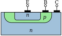
A BJT consists of three differently doped semiconductor regions, the emitter region, the base region and the collector region. These regions are, respectively, p type, n type and p type in a PNP, and n type, p type and n type in a NPN transistor. Each semiconductor region is connected to a terminal, appropriately labeled: emitter (E), base (B) and collector (C).
The base is physically located between the emitter and the collector and is made from lightly doped, high resistivity material. The collector surrounds the emitter region, making it almost impossible for the electrons injected into the base region to escape being collected, thus making the resulting value of α very close to unity, and so, giving the transistor a large β. A cross section view of a BJT indicates that the collector–base junction has a much larger area than the emitter–base junction.
The bipolar junction transistor, unlike other transistors, is usually not a symmetrical device. This means that interchanging the collector and the emitter makes the transistor leave the forward active mode and start to operate in reverse mode. Because the transistor's internal structure is usually optimized for forward-mode operation, interchanging the collector and the emitter makes the values of α and β in reverse operation much smaller than those in forward operation; often the α of the reverse mode is lower than 0.5. The lack of symmetry is primarily due to the doping ratios of the emitter and the collector. The emitter is heavily doped, while the collector is lightly doped, allowing a large reverse bias voltage to be applied before the collector–base junction breaks down. The collector–base junction is reverse biased in normal operation. The reason the emitter is heavily doped is to increase the emitter injection efficiency: the ratio of carriers injected by the emitter to those injected by the base. For high current gain, most of the carriers injected into the emitter–base junction must come from the emitter.
The low-performance "lateral" bipolar transistors sometimes used in CMOS processes are sometimes designed symmetrically, that is, with no difference between forward and backward operation.
Small changes in the voltage applied across the base–emitter terminals causes the current that flows between the emitter and the collector to change significantly. This effect can be used to amplify the input voltage or current. BJTs can be thought of as voltage-controlled current sources, but are more simply characterized as current-controlled current sources, or current amplifiers, due to the low impedance at the base.
Early transistors were made from germanium but most modern BJTs are made from silicon. A significant minority are also now made from gallium arsenide, especially for very high speed applications (see HBT, below).
Transistor Types[edit | edit source]
DC Characteristics[edit | edit source]
I - V[edit | edit source]
V I Operation V < VBE I = 0 Transistor does not conduct V = VBE I = 1mA Transistor starts conduct V > VBE I = Transistor conducts V = Vs I = Is Transistor stop conduct current . transistor saturates
Current[edit | edit source]
AC Characteristics[edit | edit source]
If apply a full Sinusoidal wave to the Base of NPN Transistor . The collector of the NPN Transistor would pass Half Positive Cycle of the Sinusoidal Wave . This introduce Harmonic in the circuit due to wavefrorm is not exactly the same from input to output
If apply a full Sinusoidal wave to the Base of PNP Transistor . The collector of the PNP Transistor would pass Half Negative Cycle of the Sinusoidal Wave . This introduce Harmonic in the circuit due to wavefrorm is not exactly the same from input to output


