Electronics/Print Version
| This is the print version of Electronics You won't see this message or any elements not part of the book's content when you print or preview this page. |
The current, editable version of this book is available in Wikibooks, the open-content textbooks collection, at
https://en.wikibooks.org/wiki/Electronics
Aim
Electronics | Foreword | Basic Electronics | Complex Electronics | Electricity | Machines | History of Electronics | Appendix | edit
The aim of this textbook is to explain the design and function of electronic circuits and components. The text covers electronic circuit components, DC analysis, and AC analysis.
It should be useful to beginner hobbyists as well as beginner engineering students, teaching both theory and practical applications.
It should be thought of as a companion project to the Wikipedia articles about electronics. While Wikipedia covers many details about the technology used in electronics components and related fields, the Electronics Wikibook covers a lot of the "how-to" aspects that aren't covered in an encyclopedia. The book will focus on how to use the components to build useful circuits.
Prereq
Electronics | Foreword | Basic Electronics | Complex Electronics | Electricity | Machines | History of Electronics | Appendix | edit
Prerequisite Topics[edit | edit source]
![]() Most important / Required knowledge
Most important / Required knowledge
![]() Moderately Important / Aids in comprehension
Moderately Important / Aids in comprehension
![]() Slightly Important / Related or helpful
Slightly Important / Related or helpful
Mathematics ![]()
Physics ![]()
Other Useful Topics
Preface
Electronics | Foreword | Basic Electronics | Complex Electronics | Electricity | Machines | History of Electronics | Appendix | edit
Importance of Electronics[edit | edit source]
Electronics is the study and use of devices that control the flow of electrons (or other charged particles). These devices can be used to process information or perform tasks using electromagnetic power.
Electronic circuits can be found in numerous household products, including such items as telephones, computers, and CD players. Electronic devices have also allowed greatly increased precision in scientific measurements.
Interest in the field of electronics increased around 1900 and the advent of radio. Interest reached an all-time high in the 1940s, 50s, 60s, with the invention of transistor radios, the launch of Sputnik, and the science and math educational push to win the space race. Interest in electronics as a hobby in the 1970s led to the advent of the personal computer (PC).
Electronics have since seen a decline in hobbyist interest. Electronics is now generally studied as part of a college-level program in electrical engineering.
This book is an attempt at reviving the hobbyist mentality that made electronics so big in the first place, by making electronics concepts more accessible and giving practical knowledge, as well as providing technical information for the student.
Charge and Coulomb's Law
Electronics | Foreword | Basic Electronics | Complex Electronics | Electricity | Machines | History of Electronics | Appendix | edit
Two atoms are walking down the street. The first atom says to the second atom "I think I lost an electron!" The second says "Are you sure?" To which the first states "I'm positive!"
Basic Understanding[edit | edit source]
- Conductors
- Materials which contain movable charges that can flow with minimal resistance.
- Insulators
- Materials with few or no movable charges, or with charges which flow with extremely high resistance.
- Semiconductors
- Materials whose behavior ranges between that of a conductor and that of an insulator under different conditions. Their conducting behavior may be heavily dependent on temperature. They are useful because we are able to change their conducting behavior to be dependent on many other factors.
- The Atom
- An atom contains a positively charged nucleus and one or more negatively charged electrons. The atom exists in three states: neutral, positively charged, and negatively charged. A neutral atom has the same number of electrons and protons, a positively charged atom has more protons than electrons and a negatively charged atom has more electrons than protons.
- (+) and (-) Ions
- An ion is an atom that has an unequal number of electrons and protons. Ions are formed when a neutral atom gains or loses electrons during a chemical reaction. In a battery, the positive side has + ions, means there are fewer electrons than protons, giving it an overall positive charge, and -ve side, more electrons than protons, giving it an overall negative charge. +ve and -ve charge will attract each other, and it is the use of such an attractive force that allows the battery to do work.
Note: Electric current is not the same as electron flow as is widely mistaken. Firstly, the total current has the opposite direction compared to electron flow. This is a lucky "mistake" on our forefathers' part to put it this way. It is also because of this lucky legacy that we are reminded that electricity can flow in materials other than metals alone. For example, in water, it is not electrons that flow, it is ions, and the +ve ions and -ve ions flow in opposite directions, contributing half of the total current each.
Balance of Charge[edit | edit source]
Atoms, the smallest particles of matter that retain the properties of the matter, are made of protons, electrons, and neutrons. Protons have a positive charge, Electrons have a negative charge that cancels the proton's positive charge. Neutrons are particles that are similar to a proton but have a neutral charge. There are no differences between positive and negative charges except that particles with the same charge repel each other and particles with opposite charges attract each other. If a solitary positive proton and negative electron are placed near each other they will come together to form a hydrogen atom. This repulsion and attraction (force between stationary charged particles) is known as the Electrostatic Force and extends theoretically to infinity, but is diluted as the distance between particles increases.
When an atom has one or more missing electrons it is left with a positive charge, and when an atom has at least one extra electron it has a negative charge. Having a positive or a negative charge makes an atom an ion. Atoms only gain and lose protons and neutrons through fusion, fission, and radioactive decay. Although atoms are made of many particles and objects are made of many atoms, they behave similarly to charged particles in terms of how they repel and attract.
In an atom the protons and neutrons combine to form a tightly bound nucleus. This nucleus is surrounded by a vast cloud of electrons circling it at a distance but held near the protons by electromagnetic attraction (the electrostatic force discussed earlier). The cloud exists as a series of overlapping shells / bands in which the inner valence bands are filled with electrons and are tightly bound to the atom. The outer conduction bands contain no electrons except those that have accelerated to the conduction bands by gaining energy. With enough energy an electron will escape an atom (compare with the escape velocity of a space rocket). When an electron in the conduction band decelerates and falls to another conduction band or the valence band a photon is emitted. This is known as the photoelectric effect.
A laser is formed when electrons travel back and forth between conduction bands emitting synchronized photons.
- When the conduction and valence bands overlap, the atom is a conductor and allows for the free movement of electrons. Conductors are metals and can be thought of as a bunch of atomic nuclei surrounded by a churning "sea of electrons".
- When there is a large energy level gap between the conduction and valence bands, the atom is an insulator; it traps electrons. Many insulators are non-metals and are good at blocking the flow of electrons.
- When there is a small energy level gap between the conduction and valence bands, the atom is a semiconductor. Semiconductors behave like conductors and insulators, and work using the conduction and valence bands. The electrons in the outer valence band are known as holes. They behave like positive charges because of how they flow. In semiconductors electrons collide with the material and their progress is halted. This makes the electrons have an effective mass that is less than their normal mass. In some semiconductors holes have a larger effective mass than the conduction electrons.
Electronic devices are based on the idea of exploiting the differences between conductors, insulators, and semiconductors but also exploit known physical phenomena such as electromagnetism and phosphorescence.
Conductors[edit | edit source]
In a metal the electrons of an object are free to move from atom to atom. Due to their mutual repulsion (calculable via Coulomb's Law ), the valence electrons are forced from the centre of the object and spread out evenly across its surface in order to be as far apart as possible. This cavity of empty space is known as a Faraday Cage and stops electromagnetic radiation, such as charge, radio waves, and EMPs (Electro-Magnetic Pulses) from entering and leaving the object. If there are holes in the Faraday Cage then radiation can pass.
One of the interesting things to do with conductors is demonstrate the transfer of charge between metal spheres. Start by taking two identical and uncharged metal spheres which are each suspended by insulators (such as a pieces of string). The first step involves putting sphere 1 next to but not touching sphere 2. This causes all the electrons in sphere 2 to travel away from sphere 1 to the far end of sphere 2. So sphere 2 now has a negative end filled with electrons and a positive end lacking electrons. Next sphere 2 is grounded by contact with a conductor connected with the earth and the earth takes its electrons leaving sphere 2 with a positive charge. The positive charge (absence of electrons) spreads evenly across the surface due to its lack of electrons. If suspended by strings, the relatively negatively charged sphere 1 will attract the relatively positively charged sphere 2.
Insulators[edit | edit source]
In an insulator the charges of a material are stuck and cannot flow. This allows an imbalance of charge to build up on the surface of the object by way of the triboelectric effect. The triboelectric effect (rubbing electricity effect) involves the exchange of electrons when two different insulators such as glass, hard rubber, amber, or even the seat of one's trousers, come into contact. The polarity and strength of the charges produced differ according to the material composition and its surface smoothness. For example, glass rubbed with silk will build up a charge, as will hard rubber rubbed with fur. The effect is greatly enhanced by rubbing materials together.
- Van de Graaff Generator: A charge pump (pump for electrons) that generates static electricity. In a Van de Graaff generator, a conveyor belt uses rubbing to pick up electrons, which are then deposited on metal brushes. The end result is a charge difference.
Because the material being rubbed is now charged, contact with an uncharged object or an object with the opposite charge may cause a discharge of the built-up static electricity by way of a spark. A person simply walking across a carpet may build up enough charge to cause a spark to travel over a centimetre. The spark is powerful enough to attract dust particles to cloth, destroy electrical equipment, ignite gas fumes, and create lightning. In extreme cases the spark can destroy factories that deal with gunpowder and explosives. The best way to remove static electricity is by discharging it through grounding. Humid air will also slowly discharge static electricity. This is one reason cells and capacitors lose charge over time.
Note: The concept of an insulator changes depending on the applied voltage. Air looks like an insulator when a low voltage is applied. But it breaks down as an insulator, becomes ionised, at about ten kilovolts per centimetre. A person could put their shoe across the terminals of a car battery and it would look like an insulator. But putting a shoe across a ten kilovolt powerline will cause a short.

Quantity of Charge[edit | edit source]
Protons and electrons have opposite but equal charge. Because in almost all cases, the charge on protons or electrons is the smallest amount of charge commonly discussed, the quantity of charge of one proton is considered one positive elementary charge and the charge of one electron is one negative elementary charge. Because atoms and such particles are so small, and charge in amounts of multi-trillions of elementary charges are usually discussed, a much larger unit of charge is typically used. The coulomb is a unit of charge, which can be expressed as a positive or negative number, which is equal to approximately 6.2415×10¹⁸ elementary charges. Accordingly, an elementary charge is equal to approximately 1.602×10⁻¹⁹ coulombs. The commonly used abbreviation for the coulomb is a capital C. The SI definition of a coulomb is the quantity of charge which passes a point over a period of 1 second ( s ) when a current of 1 ampere (A) flows past that point, i.e., C = A·s or A = C/s. You may find it helpful during later lessons to retain this picture in your mind (even though you may not recall the exact number). An ampere is one of the fundamental units in physics from which various other units are defined, such as the coulomb.
Force between Charges: Coulomb's Law[edit | edit source]
The repulsive or attractive electrostatic force between charges decreases as the charges are located further from each other by the square of the distance between them. An equation called Coulomb's law determines the electrostatic force between two charged objects. The following picture shows a charge q at a certain point with another charge Q at a distance of r away from it. The presence of Q causes an electrostatic force to be exerted on q.

The magnitude of the electrostatic force F, on a charge q, due to another charge Q, equals Coulomb's constant multiplied by the product of the two charges (in coulombs) divided by the square of the distance r, between the charges q and Q. Here a capital Q and small q are scalar quantities used for symbolizing the two charges, but other symbols such as q1 and q2 have been used in other sources. These symbols for charge were used for consistency with the electric field article in Wikipedia and are consistent with the Reference below.

F = magnitude of electrostatic force on charge q due to another charge Q
r = distance (magnitude quantity in above equation) between q and Q
k = Coulomb's constant = 8.9875×10⁹ N·m2/C2 in free space
The value of Coulomb's constant given here is such that the preceding Coulomb's Law equation will work if both q and Q are given in units of coulombs, r in metres, and F in newtons and there is no dielectric material between the charges. A dielectric material is one that reduces the electrostatic force when placed between charges. Furthermore, Coulomb's constant can be given by:

where = permittivity. When there is no dielectric material between the charges (for example, in free space or a vacuum),

Air is only very weakly dielectric and the value above for will work well enough with air between the charges. If a dielectric material is present, then


where is the dielectric constant which depends on the dielectric material. In a vacuum (free space), and thus . For air, . Typically, solid insulating materials have values of and will reduce electric force between charges. The dielectric constant can also be called relative permittivity, symbolized as in Wikipedia.


Highly charged particles close to each other exert heavy forces on each other; if the charges are less or they are farther apart, the force is less. As the charges move far enough apart, their effect on each other becomes negligible.
Any force on an object is a vector quantity. Vector quantities such as forces are characterized by a numerical magnitude (i. e. basically the size of the force) and a direction. A vector is often pictured by an arrow pointing in the direction. In a force vector, the direction is the one in which the force pulls the object. The symbol is used here for the electric force vector. If charges q and Q are either both positive or both negative, then they will repel each other. This means the direction of the electric force on q due to Q is away from Q in exactly the opposite direction, as shown by the red arrow in the preceding diagram. If one of the charges is positive and the other negative, then they will attract each other. This means that the direction of on q due to Q is exactly in the direction towards Q, as shown by the blue arrow in the preceding diagram. The Coulomb's equation shown above will give a magnitude for a repulsive force away from the Q charge. A property of a vector is that if its magnitude is negative, the vector will be equal to a vector with an equivalent but positive magnitude and exactly the opposite direction. So, if the magnitude given by the above equation is negative due to opposite charges, the direction of the resulting force will be directly opposite of away from Q, meaning the force will be towards Q, an attractive force. In other sources, different variations of Coulombs' Law are given, including vector formulas in some cases (see Wikipedia link and reference(s) below).

In many situations, there may be many charges, Q1, Q2, Q3, through Qn, on the charge q in question. Each of the Q1 through Qn charges will exert an electric force on q. The direction of the force depends on the location of the surrounding charges. A Coulomb's Law calculation between q and a corresponding Qi charge would give the magnitude of the electric force exerted by each of the Qi charges for i = 1 through n, but the direction of each of the component forces must also be used to determine the individual force vectors, . To determine the total electric force on q, the electric force contributions from each of these charges add up as vector quantities, not just like ordinary (or scalar) numbers.


The total electric force on q is additive to any other forces affecting it, but all of the forces are to be added together as vectors to obtain the total force on the charged object q. In many cases, there are billions of electrons or other charges present, so that geometrical distributions of charges are used with equations stemming from Coulomb's Law. Practically speaking, such calculations are usually of more interest to a physicist than an electrician, electrical engineer, or electronics hobbyist, so they will not be discussed much more in this book, except in the section on capacitors.
In addition to the electrostatic forces described here, electromagnetic forces are created when the charges are moving. These will be described later.
Reference(s):
- College Physics Volume 2 by Doug Davis, Saunders College Publishing, Orlando, FL, 1994
Next: Voltage, Current, and Power
Return to: Electronics Outline
Voltage, Current, and Power
Electronics | Foreword | Basic Electronics | Complex Electronics | Electricity | Machines | History of Electronics | Appendix | edit
Voltage, Current, and Power[edit | edit source]
Basic Understanding[edit | edit source]
Experiments show us that electric point charges attract or repel as calculated by Coulomb's law. Integrating (summing) over a distribution of points charges as they are assembled into a specific system configuration allows us to determine a scalar value defined as the electrical potential or electric field of a specific point. This mathematical definition is very useful in electronics circuit theory.
Voltage
- The potential difference between two test points resulting from the distribution of charge in the circuit, usually measured in volts.
Current
- Net amount of charge (coulombs) (number of electrons x electron charge) flowing past a specified point during a time interval (seconds), usually measured in Amps (1 Amp = 1 coulomb / 1 second). In typical components and systems the quantity of electrons is quite large and the aggregate charge flow is referred to as electricity.
Power
- Energy given in a certain amount of time, usually measured in watts.
Law of Charges
- Opposite charges attract while similar charges repel.
Inductance
- When electricity passes through a wire it creates a moving magnetic field around the wire. The typical unit of measure is Henrys.
Capacitance
- When electric fields or charge distributions are created in a physical system that stores recoverable energy, characteristics of the physical components which affect calculation of the electrical quantities are defined as capacitance. The base unit of measure is Farads, however microfarads (μF), are used much more often.
Resistance
- When potential difference creates movement of electrons between two points, some of the potential energy formerly available in the system is irreversibly transferred from the electric field or the electrons moving through the component via collisions with atoms and molecules within the material. Ohm's Law, V=IR, defines resistance as R=V/I where V is the voltage difference applied across the component, I is the resulting current flow in Amps, and R is a constant created by characteristics of the component which is calculated from the measured voltage loss of the measured current passing through the component.
Electric Field[edit | edit source]
A charged particle such as a proton or electron may "feel" an electrical force on it in a certain environment. This force is typically due to the presence of other charges nearby. The force will have a direction and magnitude, and can be represented by a vector. (A vector is simply a quantity that represents the direction and magnitude of something.) The magnitude of the force depends on the charge of the particle, the charge on the particles around it, and how close or far away they are: Highly charged particles close to each other exert heavy forces on each other; if the charges are less, or they are farther apart, the force is less. The direction of the force depends on the location of the surrounding charges.
In describing the electrical environment at that location , it is said there is an electric field at that location. The electric field is defined as the force that a single unit of charge would feel at that location. In some systems of measurement, the unit of charge is the charge of a single proton; in others it is the coulomb. A coulomb is the charge of 6.24×10¹⁸ protons
The relationship between force and electric field for a single charged particle is given by the following equation:

The bold letters indicate vector quantities. This means that a charge q, in an electric field E, having a certain direction and a magnitude E, would have a force F on it, in the same direction and with a magnitude F. Considering only the magnitudes, the following would result from the definition.
E = F/q these are all magnitudes or numerical quantities
The net electric field E, at a location is due to the presence of all other charges nearby, similar to the net electric force F, if there was a charge q at that location. The contribution of one of these other charges to the total (or net) electric field is a vector E contribution, which for a point charge can be derived from Coulomb's Law. Distributions of charge density in various shapes may also yield vector E contributions to the total electric field, to be added in as vector quantities. Practically speaking, most electricians, electrical engineers, and other electrical circuit builders and hobbyists seldom do these sorts of electric field calculations. Electric field calculations of this sort are more of a theoretical physics or special applications problem, so these calculations are omitted here in favor of more applicable material. See Electric Field for such information on electric field formulas.
There is an electrical force on a charge only if there is a charge subject to the force at a location in an electric field. However, even if there is no such charge subject to the force, there could still be an electric field at a point. This means that an electric field is a property of a location or point in space and its electrical environment, which would determine what a charge q would "feel" if it were there.
Energy[edit | edit source]
Now, a micro-physics review: Work is causing displacement (or movement) of an object or matter against a force. Energy is the ability to perform work like this. Energy can be kinetic energy or potential energy. Kinetic energy is the energy a mass has because it is moving. Potential energy in an object, in matter, in a charge or other situation has the ability to perform work or to be converted into kinetic energy or a different kind of potential energy.
A reason why a particle or a charge may have potential energy could be because it is located at a point in a force field, such as a gravitational field, electric field, or magnetic field. In the presence of such a field, gravity or electric or magnetic forces could cause the particle or charge to move faster or move against resistive forces, representing a conversion of potential energy to kinetic energy or work. The amount of potential energy it has would depend on its location. Moving from one location to another could cause a change in its potential energy.
For example, an object near the surface of the earth placed high would have a certain amount of gravitational potential energy based on its mass, location (height or altitude) in and strength of the Earth's gravitational field. If the object were to drop from this location (height) to a new lower location, at least some of its gravitational potential energy would be converted to kinetic energy, resulting in the object moving down. The difference in gravitational potential energy could be calculated from one location to another, but determining the absolute potential energy of the object is arbitrary, so ground level is chosen arbitrarily as the height where its gravitational potential energy equals zero. The potential energy at all other heights is determined from the mass of the object, location relative to the ground level, and strength of the gravitational field.
All energy values are numerical or scalar quantities, not vectors.
Electric Potential Energy[edit | edit source]
Somewhat similarly, a charged particle at a certain point or location in an electrical environment (i. e. an electric field) would have a certain amount of electric potential energy based on its charge, location, and the electric field there, which could be based on quantity and locations of all other charges nearby. If the charge were to move from this location to a new location or point, it could cause a change in its electric potential energy. This difference in electric potential energy in the charge particle would be proportional to its charge and it could be an increase or a decrease. From measurements and calculations, one may be able to determine this difference in electric potential energy, but coming up with an absolute figure for its potential is difficult and typically not necessary. Therefore, in a manner somewhat similar to gravitational potential energy, an arbitrary location or point nearby, often somewhere in the electric circuit in question, is chosen to be the point where the electric potential energy would be zero, if the charge were there. Often the wiring, circuit, or appliance will be connected to the ground, so this ground point is often chosen to be the zero point. The electric potential energy at all other points is determined relative to the ground level. The SI unit of electric potential energy is the joule.
Electric Potential[edit | edit source]
Because the electric potential energy of a charged particle (or object) is proportional to its charge and otherwise simply dependent on its location (point where it's at), a useful value to use is electric potential. Electric potential (symbolized by V) at a point is defined as the electric potential energy (PE) per unit positive charge (q) that a charge would have at that given point (location). At a point a, the electric potential at a is given by:
Va = (PE of charge at a)/q
Somewhat analogously to an electric field, electrical potential is a property of a location and the electrical conditions there, whether or not there is a charge present there subject to these conditions. On the other hand, electric potential energy is more analogous to electric force in that for it to be present, there should be a subject charged particle or object which has that energy. Electric potential is often simply called potential by physicists. Because the SI unit of electric potential energy is the joule and because the SI unit of charge is the coulomb, the SI unit for electric potential, the volt (symbolized by V), is defined as a joule per coulomb (J/C).
Because electric potential energy is based on an arbitrary point where its value is set at as zero, the value of electric potential at a given point is also based on this same arbitrary zero point (reference point where the potential is set at zero). The potential at a given point a is then the difference between potentials from point a to the zero point, often called a ground node (or just ground).
Calculations of electric potential energy or electric potential based on Coulomb's Law are sometimes theoretically possible, such as might be for electric field calculations, but again these are of mostly theoretical interest and not often done in practical applications. Therefore, such calculations are also omitted here in favour of more applicable material.
Often it is of interest to compare the potentials at two different points, which we may call point a and point b. Then the electric potential difference between points a and b (Vab) would be defined as the electric potential at b minus the electric potential at a.
Vab = Vb - Va
The unit for electric potential difference is the volt, the same as for electric potential. Electric potential difference is often simply called potential difference by physicists. Under direct current (DC) conditions and at any one instant in time under alternating current (AC), potential and potential difference are numerical or scalar quantities, not vectors, and they can have positive or negative values.
Voltage[edit | edit source]
Voltage is electric potential expressed in volts. Similarly, potential difference expressed in volts is often called voltage difference or often referred to as voltage across two points or across an electrical component. The terms electric potential, potential, and potential difference are terms more often used by physicists. Since these quantities are almost always expressed in volts (or some related unit such as millivolts), engineers, electricians, hobbyists, and common people usually use the term voltage instead of potential. Furthermore, in practical applications, electrical force, electric field, and electrical potential energy of charged particles are not discussed nearly as often as voltage, power, and energy in a macroscopic sense.
Additional note: The following explains why voltage is "analogous" to the pressure of a fluid in a pipe (although, of course, it is only an analogy, not exactly the same thing), and it also explains the strange-sounding "dimensions" of voltage. Consider the potential energy of compressed air being pumped into a tank. The energy increases with each new increment of air. Pressure is that energy divided by the volume, which we can understand intuitively. Now consider the energy of electric charge (measured in coulombs) being forced into a capacitor. Voltage is that energy per charge, so voltage is analogous to a pressure-like sort of forcefulness. Also, dimensional analysis tells us that voltage ("energy per charge") is charge per distance, the distance being between the plates of the capacitor. (More discussion is on page 16 of "Industrial Electronics," by D. J. Shanefield, Noyes Publications, Boston, 2001.)
Frequency[edit | edit source]
When an electric circuit is operating in Direct Current (DC) mode, all voltages and voltage differences in the circuit are typically constant (do not vary) with time. When a circuit is operating under Alternating Current (AC) conditions, the voltages in the circuit vary periodically with time; the voltages are a sinusoidal function of time, such as V(t) = a sin (b t) with constant a and b, or some similar function. The number of times the period repeats (or "cycles") per unit time is called the frequency of V(t). Under DC conditions or at any one instant in time under AC, potential (or voltage) and potential difference (or voltage difference) are numerical or scalar quantities, not vectors, and they can have positive or negative values. However, in AC mode, the overall function of voltage with time V(t), can be expressed as a complex number or a phasor for a given frequency. The frequency can be expressed in cycles per second or simply sec-1, which is called Hertz (Hz) in SI units. Typical commercial electric power provided in the United States is AC at a frequency of 60 Hz (50 Hz for India).
Ground[edit | edit source]
Ground is shown on electronics diagrams, but it isn't really a component. It is simply the node which has been assigned a voltage of zero. It is represented by one of the symbols below. Technically, any single node can be assigned as ground, and other voltages are measured relative to it. However, the convention is to only assign it in one of two ways, related to the type of power supply. In a single supply situation, such as a circuit powered by a single battery, the ground point is usually defined as the more negative of the power source's terminals. This makes all voltages in the circuit positive with respect to ground (usually), and is a common convention. For a split-supply device, such as a circuit driven by a center-tapped transformer, usually the center voltage is defined as ground, and there are equal and roughly symmetrical positive and negative voltages in the circuit.
| Signal Ground |
Chassis Ground |
Earth Ground |
- Signal ground
- Ground for a signal. Since wires have a certain amount of resistance to them, ground points in a circuit aren't all at exactly the same voltage. It is important in practical circuit design to separate the power supply ground from the signal ground from the shielding ground, etc. In circuits where minimum noise is especially important, power regulator circuitry should have thick wires or traces connecting the grounds, in a sequence from the power supply to the "cleanest" ground at the output of the filters of the power supply, which will then be a "star point" for the grounds of the signal circuitry.
- Chassis ground
- A direct connection to the chassis of the device. This is used for EMI shielding and also for safety ground in line AC powered devices.
- Earth ground
- Used in radio or power distribution systems, a connection to the earth itself. Also the other end of the connection for the safety ground, since the power line voltage will seek a path through the earth back to the power line supply station. This was the original usage of the word "ground", and the more modern meaning of the word would have been called a "floating ground".
The earth ground symbol and signal ground symbol are often interchanged without regard to their original meanings. As far as signal-level electronics (and this book) is concerned, ground almost always means a signal ground or floating ground, not connected to the earth itself.
(see: http://www.prosoundweb.com/studyhall/rane/grounding/ground2.php)
Current[edit | edit source]
Electric current, often called just current, is the movement of charge in a conductor (such as a wire) or into, out of, or through an electrical component. Current is quantified as a rate of positive charge movement past a certain point or through a cross-sectional area. Simply put, current is quantified as positive charge per unit time. However, since current is a vector quantity, the direction in which the current flows is still important. Current flow in a given direction can be positive or negative; the negative sign means that positive charges move opposite of the given direction. The quantity of current at a certain point is typically symbolized by a capital or small letter I with a designation which direction the current I is moving. The SI unit of current is the ampere (A), one of the fundamental units of physics. See ampere for the definition of ampere. Sometimes, ampere is informally abbreviated to amp. The definition of a coulomb (C), the SI unit of charge, is based on an ampere. A coulomb is the amount of positive charge passing a point when a constant one ampere current flows by the point for one second. The second is the SI unit of time. In other words, a coulomb equals an ampere-second (A·s). An ampere is a coulomb per second (C/s).
Conventional Current[edit | edit source]
Typically, current is in a metal and constitutes movement of electrons which have negative charge; however, people initially thought that current had a positive charge. The result is that even though current is the flow of negative electrons and flows from the negative to the positive terminal of a battery, when people do circuit analysis they pretend that current is a flow of positive particles and flows from the positive to the negative terminal of a battery (or other power source). Actually, it is more complicated than this, since current can be made up of electrons, holes, ions, protons, or any charged particle. Since the actual charge carriers are usually ignored when analyzing a circuit, current is simplified and thought of as flowing from positive to negative, and is known as conventional current.
Analogy to pebble tossing: I have pebbles and I am throwing them into a basket. In doing this the basket gains pebbles and I lose pebbles. So there is a negative current of pebbles to the basket because it is gaining pebbles, and there is a positive current of pebbles to me because I am losing pebbles. In pebble tossing the currents have equal strength but in opposite directions.
Current I is represented in amperes (A) and equals x number of y
Power[edit | edit source]
Power is energy per unit of time. The SI unit for power is the watt (W) which equals a joule per second (J/s), with joule being the SI unit for energy and second being the SI unit for time. When somebody plugs an appliance into a receptacle to use electricity to make that appliance function, that person provides electrical energy for the appliance. The appliance usually functions by turning that electrical energy into heat, light, or work — or perhaps converts it into electrical energy again in a different form. If this situation is ongoing, it is said that the receptacle or electric power company delivers power to the appliance. The current from the receptacle going in and out of the appliance effectively carries the power and the appliance absorbs the power.
Multiplying a unit of power by a unit of time would result in a unit that represents a quantity of energy. Therefore, multiplying a kilowatt by an hour gives a kilowatt-hour (kW·h), a unit often used by electrical power companies to represent an amount of electrical energy generated or provided to consumers. Oddly, in marketing and retail packaging, portable batteries are often rated in "mAh", which are normally units of power, but do not identify how much power the battery can supply. Rather, the mAh rating is always at the implied voltage defined by the battery's chemistry. For example, a common, premium quality 18650 Li-ion battery would be advertised/rated 3400 mAh, at most. Even though "3400 mAh" is in power units, Li-ion chemistry battery voltage is typically around 3.7 volts, and this does identify the battery as one that should be able to store about 3400 mAh x 3.7 volts = 12.6 mWh (milliwatt hours) of energy per charge.) Also oddly, in marketing and retail packaging, a larger (e.g. vehicle) battery is often advertised based on the "Amps" or "Cold Cranking Amps" (CCA) the battery can provide to indicate the maximum power it can deliver. Although Amps are not power units, these ratings do represent the amount of power that can be output.
For direct current (DC), power P can be calculated by multiplying the voltage and current, when they are known.
P = V I
Note that energy/charge is multiplied by charge/time to give energy/time. At any one point in time t in alternating current (AC) circuitry, power P(t) equals voltage V(t) times current I(t).
P(t) = V(t) I(t) at any one time t
Calculations of AC power averaged over time will be discussed under AC power.
Circuit[edit | edit source]
An electronic circuit is a system in which conventional current flows from the positive terminal of a source, through a load, to the negative terminal of the source. But the current will only flow when there is a closed path from the positive to negative terminal. If there is a discontinuity or an open circuit in its path, the current will not flow and hence the circuit will be non functional. The current does not flow since the open circuit acts like an infinite resistance.
Short Circuit[edit | edit source]
![]()
A short circuit is another name for a node, although it usually means an unintentional node. Has current through it but no voltage across it.
Open Circuit[edit | edit source]
![]()
Has potential across it but no current through it.
Properties of wires[edit | edit source]
Theoretical circuit connection (wire) has no resistance or inductance. Real wires always have voltage over them if there is current flowing through them (resistance). On high frequencies there are measurable voltage potentials over wire links if there is flowing alternating current through wires (inductance like in inductors).
Basic Concepts
What is Electronics?[edit | edit source]
Electronics is the study of flow of electrons in various materials or space subjected to various conditions. In the past, electronics dealt with the study of Vacuum Tubes or Thermionic valves, today it mainly deals with flow of electrons in semiconductors. However, despite these technological differences, the main focus of electronics remains the controlled flow of electrons through a medium. By controlling the flow of electrons, we can make them perform special tasks, such as power an induction motor or heat a resistive coil.
Plumbing Analogy: A simple way to understand electrical circuits is to think of them as pipes. Let's say you have a simple circuit with a voltage source and a resistor between the positive and negative terminals on the source. When the circuit is powered, electrons will move from the negative terminal, through the resistor, and into the positive terminal. The resistor is basically a path of conduction that resists the movement of electrons. This circuit could also be represented as a plumbing network. In the plumbing network, the resistor would be equivalent to a section of pipe, where the water is forced to move around several barriers to pass through, effectively slowing its flow. If the pipe is level, no water will flow in an organized fashion, since the pressure is equal throughout the pipe. However, if we tilt the pipe to a vertical position (similar to turning on a voltage source), a pressure difference is created (similar to a voltage difference) and the water begins flowing through the pipe. This flow of water is similar to the flow of electrons in a circuit.
Electricity[edit | edit source]
To understand electronics, you need to understand electricity and what it is. Basically, electricity is the flow of electrons due to a difference in electrical charge between two points. This difference in charge is created due to a difference in electron density. If you have a point where the electron density is higher than the electron density at another point, the electrons in the area of higher density will want to balance the charge by migrating towards the area with lower density. This migration is referred to as electrical current. Thus, flow in an electrical circuit is induced by putting more electrons on one side of the circuit than the other, forcing them to move through the circuit to balance the charge density.
Electric Charge[edit | edit source]
Observations tell us that matter can either be electrically neutral (that is, have no net charge), or carry a positive or negative charge. On a microscopic level, a negative charge corresponds to an excess of electrons in the material (which each carry a 'unit' of negative charge), and a positive charge a shortage of electrons. We denote the charge of an object by , which is measured in Coulombs.

Coulomb's Law[edit | edit source]
Two objects that have the same type of charge are known to repel, whereas objects with opposite charges attract. The force between charged objects is given by Coulomb's Law:

where and are the charges of the two objects (positive or negative), is the distance between them, and a universal constant.


Electric field[edit | edit source]
Suppose we have a fixed particle (or a collection of fixed particles), then we can calculate the force on any given (test) particle with charge by applying Coulomb's Law. There is a force at any point in space; we say that there is an electric field due to the (fixed) charges. The field at any point is equal to the net force on a charged particle divided by its charge, or:


Lorentz's Law[edit | edit source]
When a charge in motion passes through a magnetic field, the magnetic field will push a positive charge upward and negative charge downward in the direction perpendicular to the initial direction traveled. The magnitude of the magnetic force on the charge is given by Lorentz's Law:

Electromagnetic Force[edit | edit source]
The sum of the Coulomb and Lorentz's Forces is called the ElectroMagnetic Force:

Electricity and Matter[edit | edit source]
All matter interacts with Electricity, and are divided into three categories: Conductors, Semi Conductors, and Non Conductors.
- Matter that conducts Electricity easily. Metals like Zinc (Zn) and Copper (Cu) conduct electricity very easily. Therefore, they are used to make Conductors.
- Matter that does not conduct Electricity at all. Non-Metals like Wood and Rubber do not conduct electricity so easily. Therefore, they are used to make Non-Conductors.
- Matter that conducts electricity in a manner between that of Conductors and Non-Conductors. For example, Silicon (Si) and Germanium (Ge) conduct electricity better than non-conductors but worse than conductors. Therefore, they are used to make Semi Conductors.
Electricity and Conductors[edit | edit source]
Normally, all conductors have a zero net charge . If there is an electric force that exerts a pressure on the charges in the conductor to force charges to move in a straight line result in a stream of electric charge moving in a straight line
Voltage[edit | edit source]
- The pressure the electric force exert on the charges is called voltage denoted as V measured in Volt (V) and defined as the ratio of Work Done on Charge


Current[edit | edit source]
- The moving of straight lines of electric charges in the conductor is called current denoted as I measured in Ampere (A) and defined as Charge flow through an area in a unit of time

Conductance[edit | edit source]
- Conductance is defined as the ratio of current over voltage denoted as Y measured in mho
- or siemens (S)

Resistance[edit | edit source]
- Resistance is defined as the ratio of voltage over current denoted as R measured in Ohm

Generally, resistance of any conductor is found to increase with increasing temperature
For Conductor
- R = Ro(1 + nT)
For Semi Conductor
- R = Ro enT
When a conductor conducts electricity, it dissipates heat energy into the surrounding . This results in a loss of electric energy transmitted. If the electric supply energy is PV and the electric loss energy is PR Then the electric energy delivered:
- P = PV - PR


Black Body Radiation[edit | edit source]
Further experience with conductors that conduct electricity . It is observed that all conductors that conduct electricity exhibit
- Change in Temperature
- Release Radiant Heat Energy into the surrounding
Experiment[edit | edit source]
Connect a conductor with an electric source in a closed loop . Plot the value I at different f to have a I - f diagram
Observation[edit | edit source]
for f<fo
- Current increasing with increasing f .
- Radiant heat is a wave travels at velocity v = λf carries energy E = m v2 .
for f=fo,
- Current stops increasing .
- Radiant heat is a wave travels at velocity v = c (speed of Light) carries energy E = hfo .
for f>fo,
- Current remains at the value of current at fo .
- Radiant heat is a wave travels at velocity v = c (speed of Light) carries energy E = h nfo
Conclusion[edit | edit source]
- All conductor that conducts Electricity has a threshold frequency fo
- The Radiant Heat Energy is a Light Wave of dual Wave Particle characteristic. Sometimes it behaves like Particle, sometimes it behaves like Wave
- At Frequency f > fo . The energy of the Light is quantized . it can only have the value of multiple integer of fo . E = hf = h nfo
Cells
Electronics | Foreword | Basic Electronics | Complex Electronics | Electricity | Machines | History of Electronics | Appendix | edit
Cells[edit | edit source]
A cell, or electrochemical cell, Galvanic cell or Voltaic cell, is a component used to store and provide electrical energy. The energy in a cell is stored as a chemical potential energy, and electrical energy can be extracted when the chemicals undergo a chemical reaction. A battery is the term used to refer to multiple cells that are used together as one unit, and can be connected in series, parallel or in a combination of series and parallel connections.
The properties of the cell can be determined by the chemistry of the cell (i.e. what it is made up of), and its physical design. Different chemistries will affect cell voltage, energy density, internal resistivity, and other factors. Physical design will affect the total cell energy capacity, total internal resistance and the shape and size of the cell. Generally, increasing the size of a cell, while maintaining the cell chemistry, will result in a greater energy capacity and lower internal resistance, and consequently a greater current supplying capability, and vice versa.
Cells are categorised as Primary (Dry) cells, and Secondary (Wet) cells, based on their chemistry. Primary cells are single-use and disposable, for example alkaline cells. Secondary cells are rechargeable, for example lead-acid cells.

- Cell: Two materials with a voltage difference between them. This causes current to flow, which does work. Electrons travel from the cathode, do some work, and are absorbed by the anode.
- Anode: Destination of electrons.
- Cathode: Source of electrons.
- ions: An atom with an imbalance of electrons.
- cell operation: The cell runs and electrons are depleted at the cathode and accumulate at the anode. This creates a reverse voltage which stops the flow of electrons.
- irreversible: At some point the voltage difference reactions between the cathode and anode will decrease to a point that the cell in unusable. At this point, in an irreversible cell, the voltage difference is irreplaceably lost, and the cell is of no further use.
- reversible: Able to run the cell backwards.
- rechargeable: In a rechargeable cell, when the voltage difference between the cathode and anode decreases, the cell can be recharged, thereby increasing the voltage difference to a suitable level to allow continued use.
- humid air will discharge cells.
- cells are usually made of toxic or corrosive substances, for example lead and sulphuric acid. Such substances have been known to explode.
- Electronegativity [16]
What is the relationship between voltage and electronegativity?
- Electronegativity is a concept in chemistry used to measure and predict the relative likelihood of a chemical reaction causing electrons to shift from one chemical to another resulting in ions and molecular bonds. A battery cell operates by allowing two chemicals to react and supply ions to the anode and cathode. When the supply of a reactant is consumed, the battery is dead. It no longer produces different electrical potential at the anode and cathode driven by the chemical reaction.
- Voltage is the electrical potential of a point due to surrounding measurable electric charge distributions and points as calculated by application Coulomb's Law. Voltage difference between two points connected by a conductor results in electron flow.
Resistors
Electronics | Foreword | Basic Electronics | Complex Electronics | Electricity | Machines | History of Electronics | Appendix | edit
Resistor[edit | edit source]

A resistor is a block or material that limits the flow of current. The greater the resistance, the lower the current will be, assuming the same voltage imposed on the resistor. The hydraulic analogy of a resistor would be the pipe with water flowing through it. The wider the diameter of a pipe, the higher the water flow through the pipe, assuming the same pressure difference on the terminals of a pipe.
Resistor's Symbol[edit | edit source]
Resistors have two leads (points of contact) to which the resistor can be connected to an electrical circuit. A symbol for a resistor used in electrical circuit diagrams is shown below.
The endpoints at the left and right sides of the symbol indicate the points of contact for the resistor. The ratio of the voltage to current will always be positive, since a higher voltage on one side of a resistor is a positive voltage, and a current will flow from the positive side to the negative side, resulting in a positive current. If the voltage is reversed, the current is reversed, leading again to a positive resistance.
Resistance[edit | edit source]
Resistance is a characteristic of Resistor indicates the measurement of current opposition . Resistance has a symbol R measured in Ohm (Ω) . The ratio of voltage to current is referred to as Ohm's Law, and is one of the most basic laws that govern electronics.
An ohm is the amount of resistance which passes one ampere of current when a one volt potential is placed across it. (The ohm is actually defined as the resistance which dissipates one watt of power when one ampere of current is passed through it.)

Resistance can vary from very small to very large. A superconductor has zero resistance, while something like the input to an op-amp can have a resistance near 1012 Ω, and even higher resistances are possible.
Resistance and Temperature[edit | edit source]
For most materials, resistance increases with increasing Temperature
- For Conductor .
- For Semi Conductor .


Resistance and Electric Power Loss[edit | edit source]
Resistance converts Electrical Energy into Heat this causes Electric Energy Loss.

NOTE : Resistors which dissipate large amounts of power are cooled so that they are not destroyed, typically with finned heatsinks.
If Electric Energy Supply is Pv and Electric Energy Loss is Pr Then, Electric Energy Delivered is


The ratio of Electric Energy Delivered over Electric Energy Supplied indicates the Efficiency of Electric Power Supply


Resistor's Labeling (See also Identification)[edit | edit source]
A manufactured resistor is usually labeled with the nominal value (value to be manufactured to) and sometimes a tolerance. Rectangular resistors will usually contain numbers that indicate a resistance and a multiplier. If there are three or four numbers on the resistor, the first numbers are a resistance value, and the last number refers to the number of zeroes in the multiplier. If there is an R in the value, the R takes the place of the decimal point.
- Examples
- 2003 means 200×103 = 200kΩ
- 600 means 60×100 = 60Ω
- 2R5 means 2.5Ω
- R01 means 0.01Ω
Cylindrical resistors (axial) usually have colored bands that indicate a number and a multiplier. Resistance bands are next to each other, with a tolerance band slightly farther away from the resistance bands. Starting from the resistance band side of the resistor, each colour represents a number in the same fashion as the number system shown above.
Colour System
Black Brown Red Orange Yellow Green Blue Violet Grey White 0 1 2 3 4 5 6 7 8 9
Clue : B.B.ROY of Great Britain was a Very Good Worker. Additional Colours: A gold band in the multiplier position means 0.1, but means a 5% tolerance in the tolerance position. A silver band in the multiplier position means 0.01, but means 10% in the tolerance position.
Resistor's Construction[edit | edit source]
The resistance R of a component is dependent on its physical dimension and can be calculated using:

where
- ρ is the electrical resistivity (resistance to electricity) of the material,
- L is the length of the material
- A is the cross-sectional area of the material.
If you increase ρ or L you increase the resistance of the material, but if you increase A you decrease the resistance of the material.
Resistivity of the Material[edit | edit source]
Every material has its own resistivity, depending on its physical makeup. Most metals are conductors and have very low resistivity; whereas, insulators such as rubber, wood, and air all have very high resistivity. The inverse of resistivity is conductivity, which is measured in units of Siemens/metre (S/m) or, equivalently. mhos/metre.
In the following chart, it is not immediately obvious how the unit ohm-meter is selected. Considering a solid block of the material to be tested, one can readily see that the resistance of the block will decrease as its cross-sectional area increases (thus widening the conceptual "pipe"), and will increase as the length of the block increases (lengthening the "pipe"). Given a fixed length, the resistance will increase as the cross-sectional area decreases; the resistance, multiplied by the area, will be a constant. If the cross-sectional area is held constant, as the length is increased, the resistance increases in proportion, so the resistance divided by the length is similarly a constant. Thus the bulk resistance of a material is typically measured in ohm meters squared per meter, which simplifies to ohm - meter (Ω-m).
Conductors Ω-m (Ohm-meter) Silver 1.59×10⁻⁸ Copper 1.72×10⁻⁸ Gold 2.44×10⁻⁸ Aluminum 2.83×10⁻⁸ Tungsten 5.6×10⁻⁸ Iron 10×10-8 Platinum 11×10-8 Lead 22×10-8 Nichrome 1.50×10⁻⁶ (A nickel-chromium alloy commonly used in heating elements) Graphite ~10-6 Carbon 3.5×10⁻⁵ Semiconductors Pure Germanium 0.6 Pure Silicon 640 Common purified water ~103 Ultra-pure water ~105 Pure Gallium Arsenide ~106 Insulators Diamond ~1010 Glass 1010 to 1014 Mica 9×10¹³ Rubber 1013 to 1016 Organic polymers ~1014 Sulfur ~1015 Quartz (fused) 5 to 75×1016 Air very high
Silver, copper, gold, and aluminum are popular materials for wires, due to low resistivity. Silicon and germanium are used as semiconductors. Glass, rubber, quartz crystal, and air are popular dielectrics, due to high resistivity.
Many materials, such as air, have a non-linear resistance curve. Normal undisturbed air has a high resistance, but air with a high enough voltage applied will become ionized and conduct very easily.
The resistivity of a material also depends on its temperature. Normally, the hotter an object is, the more resistance it has. At high temperatures, the resistance is proportional to the absolute temperature. At low temperatures, the formula is more complicated, and what counts as a high or low temperature depends on what the resistor is made from. In some materials the resistivity drops to zero below a certain temperature. This is known as superconductivity, and has many useful applications.
(Some materials, such as silicon, have less resistance at higher temperatures.)
For all resistors, the change in resistance for a small increase in temperature is directly proportional to the change in temperature.
Current passing through a resistor will warm it up. Many components have heat sinks to dissipate that heat. The heatsink keeps the component from melting or setting something on fire.
Length[edit | edit source]
The length of an object is directly proportional to its resistance. As shown in the diagram below, 1 unit cubed of material has 1 ohm of resistance. However, when 4 units are stacked lengthwise and a connection is made to the front and back sides respectively, the total resistance is 4 ohms. This is because the length of the unit is 4, whereas the cross-sectional area remains 1. However, if you were to make connections on the sides, the exact opposite would be true: the cross-sectional area would be 4 and the length 1, resulting in 0.25 ohms total resistance.

Cross-Sectional Area[edit | edit source]
Increasing area is the same as having resistors in parallel, so as you increase the area you add more paths for current to take.
The resistance of a material is inversely proportional to its cross-sectional area. This is shown in the diagram below, where 1 unit cubed has one ohm of resistance. However, if 4 units cubed are stacked on top of each other in the fashion such that there is 4 units squared of cross-sectional area, and the electrical connections are made to the front and back such that the connections are on the largest sides, the resultant resistance would be 0.25 ohms.
Additional note: There are two reasons why a small cross-sectional area tends to raise resistance. One is that the electrons, all having the same negative charge, repel each other. Thus there is resistance to many being forced into a small space. The other reason is that they collide, causing "scattering," and therefore they are diverted from their original directions. (More discussion is on page 27 of "Industrial Electronics," by D. J. Shanefield, Noyes Publications, Boston, 2001.)

Example[edit | edit source]
For instance, if you wanted to calculate the resistance of a 1 cm high, 1 cm wide, 5 cm deep block of copper, as shown in the diagram below:
![]()
You would first need to decide how it's oriented. Suppose you want to use it from front to back (lengthwise), like a piece of wire, with electrical contacts on the front and rear faces. Next you need to find the length, L. As shown, it is 5 cm long (0.05 m). Then, we look up the resistivity of copper on the table, 1.6×10⁻⁸ Ω-meters. Lastly, we calculate the cross-sectional area of the conductor, which is 1 cm × 1 cm = 1 cm2 (0.0001 m2). Then, we put it all in the formula, converting cm to m:

units m2 cancel:

Which, after evaluating, gives you a final value of 8.0×10⁻⁶ Ω, or 8 microohms, a very small resistance. The method shown above included the units to demonstrate how the units cancel out, but the calculation will work as long as you use consistent units.
- Internet Hint: Google calculator can do calculations like this for you, automatically converting units. This example can be calculated with this link: [17]
Properties of the material[edit | edit source]
- Wirewound: Used for power resistors, since the power per volume ratio is highest. These usually have the lowest noise.
- Carbon Film: These are easy to produce, but usually have lots of noise because of the properties of the material.
- Metal Film: These resistors have thermal and voltage noise attributes that are between carbon and wirewound.
- Ceramic: Useful for high frequency applications.
Resistor Connection[edit | edit source]
Resistors in Series[edit | edit source]
Resistors in series are equivalent to having one long resistor. If the properties of two resistors are equivalent, except the length, the final resistance will be the sum of the two construction methods:

This means that the resistors add when in series.

- Christmas tree lights are usually connected in series, with the unfortunate effect that if one light blows, the others will all go out (This happens because the circuit is not complete, if a circuit is not complete then the current cannot flow, hence the light bulbs all go out). However, most modern Christmas light strings have built in shunt resistors in parallel to the bulb, so that current will flow past the blown light bulb.
Resistors in Parallel[edit | edit source]
In a parallel circuit, current is divided among multiple paths. This means that two resistors in parallel have a lower equivalent resistance than either of the parallel resistors, since both resistors allow current to pass. Two resistors in parallel will be equivalent to a resistor that is twice as wide:

Since conductances (the inverse of resistance) add in parallel, you get the following equation:

For example, two 4 Ω resistors in parallel have an equivalent resistance of only 2 Ω.
To simplify mathematical equations, resistances in parallel can be represented with two vertical lines "||" (as in geometry). For two resistors the parallel formula simplifies to:

Combinations of series and parallel[edit | edit source]

Resistors in parallel are evaluated as if in a mathematical set of "parentheses." The most basic group of resistors in parallel is evaluated first, then the group in series with the new equivalent resistor, then the next group of resistors in parallel, and so on. For example, the above portion would be evaluated as follows:

Resistor variations[edit | edit source]
- Variable Resistor or Potentiometer
- Variable resistors are tunable, meaning you can turn a dial or slide a contact and change the resistance. They are used as knobs to control the volume of a stereo, or as a dimmer for a lamp. The term Potentiometer is often abbreviated as 'pot'. It is constructed like a resistor, but has a sliding tap contact. Potentiometers are used as Voltage Dividers. It is rare to find a variable resistor with only two leads. Most are potentiometers with three leads, even if one is not connected to anything.
- Rheostat
- A variation of the potentiostat with a high current rating, which is used to control the amount of power going through a load, such as a motor.
- Thermistor
- Temperature-sensitive resistor, in which the resistance decreases as the temperature rises. They are used in fire alarms, so if things get too hot the current rises and trips a switch that sounds an alarm.
- LDR (Light Dependent Resistor) or Photoresistor
- A resistor which changes values depending on the amount of light shining on its surface. The resistance decreases as the amount of light increases. They are used in street lamps, so when it gets dark the current decreases and turns on the street lamp.
Applications[edit | edit source]
- Voltage division / Attenuation: Sometimes a voltage will be too large to measure, so a means to linearly reduce the voltage is required. Placing two resistors in series to ground will provide a point in the middle to tap. Resistor RA is placed between the input voltage and the output node, and the resistor RB is placed between the output node and ground. This creates a voltage divider to lessen the output voltage. Typically, the resistors are near the value of ~10kΩ. The Thevenin model of the circuit gives an output resistance ROUT = RA||RB. A larger output resistance will more likely be affected by the input resistance of the measuring circuit (this is a desired effect in the transistor biasing circuits). Placement of the voltage divider should be close to the measuring circuit, to minimize noise (in this arrangement, it will be also lessened Rb/(Ra + Rb) times). The output voltage of the voltage divider is

- Pull-up / Pull-down: If there is nothing to drive a signal node, the node will be left "floating" (for example, such a situation occurs at the trigger input of a car alarm system when the driver has switched off the internal lamp). This may lead to unintended values being measured, or causing side-effects when the voltage is propagated down the remainder of the circuit. To prevent this, a relatively high value resistor (usually ~10kΩ to ~1MΩ) is placed between the node and ground (pull-down) or a high voltage (pull-up) to bring the voltage of the "floating" node near to the voltage it is being pulled. A resistive voltage divider is another example where the upper resistor "pulls" the output point up toward the input voltage while the lower resistor "pulls" the output point toward the ground. This idea is evolved in the circuit of a resistive voltage summer (for example, the resistors R1 and R2 of an op-amp inverting amplifier) supplied by two voltages (VIN and -VOUT) having opposite polarities. The two voltage sources "pull" the output point in opposite directions; as a result, if R2/R1 = -VOUT/VIN, the point becomes a virtual ground. Placement of a pull-up or pull-down resistor does not have a significant effect on the performance of the circuit, if they have high resistances.
- Current limiting / Isolation: In order to protect circuits from conditions that may cause too much current in a device, a current limiting resistor is inserted in the middle of the circuit. A digital input to a microcontroller may benefit from a current limiting resistor. The inputs to modern microcontrollers have protection circuitry built in that will protect the input from an overvoltage condition, provided that the current is small enough. For instance, a common microcontroller will be capable of withstanding 20mA. If there are 12V nets on a circuit board, or in a system, the digital input will benefit from a 350Ω resistor (refer to calculation below). Usually a slightly larger resistance is used in practice, but too large of a resistor will cause noise, and may prevent the input from being able to read the voltage. It is good practice to place the resistor as close as possible to the microcontroller input, so that an accidental short on the board will mean that the microcontroller input is likely still protected.

- Line termination / Impedance matching: The properties of an electric wave propagating through a conductor (such as a wire) create a reflection, which can be viewed as unwanted noise. A reflection can be eliminated by maximizing the power transfer between the conductor and the termination resistor. By matching the resistance (more importantly the impedance ), the wave will not cause a reflection. The voltage of the echo V_r is calculated below in reference to the original signal V_o as a function of the conductor impedance Z_C and the terminator impedance Z_T. As the name implies, the termination resistor goes at the end of the conductor.

- Current sensing: Measurement of a current cannot be done directly. There are three major ways to measure a current: a resistor, a hall sensor, and an inductor. The hall sensor and inductor use a property of the magnetic field to sense the current through a nearby conductor. According to Ohm's law, if a current I flows through a resistor R, a voltage V = R.I appears across the resistor. Therefore, the resistor can act as a passive current-to-voltage converter. In this arrangement, the resistor should have a very low value (sometimes on the order of ~0.01Ω), so it does not affect the current flow or heat up; however, a smaller value has a lower voltage to read, which means more noise may be introduced. This contradiction is solved in the circuit of an active current-to-voltage converter where the resistor may have a significant resistance as an op-amp compensates the "undesired" voltage drop across it (unfortunately, this remedy may be applied only in low-current measurements). The current sense resistor should be placed as close as possible to where the measurement occurs, in order not to disturb the circuit.
- Filtering: Filtering is discussed later, after an introduction to capacitors and inductors. Filters are best placed close to where measurement takes place.
Specifications[edit | edit source]
Resistors are available as pre-fabricated, real-world components. The behavior of such components deviates from an ideal resistor in certain ways. Therefore, real-world resistors are not only specified by their resistance, but also by other parameters. In order to select a manufactured resistance, the entire range of specifications should be considered. Usually, exact values do not need to be known, but ranges should be determined.
Nominal Resistance[edit | edit source]
The nominal resistance is the resistance that can be expected when ordering a resistor. Finding a range for the resistance is necessary, especially when operating on signals. Resistors do not come in all of the values that will be necessary. Sometimes resistor values can be manipulated by shaving off parts of a resistor (in industrial environments this is sometimes done with a LASER to adjust a circuit), or by combining several resistors in series and parallel.
Available resistor values typically come with a resistance value from a so called resistor series. Resistor series are sets of standard, predefined resistance values. The values are actually made up from a geometric sequence within each decade. In every decade there are supposed to be resistance values, with a constant step factor. The standard resistor values within a decade are derived by using the step factor


![{\displaystyle i={\sqrt[{n}]{10}};n=6,12,24,48}](https://wikimedia.org/api/rest_v1/media/math/render/svg/733c32c906ec24627c4ebac7b52f828cd15d8c8a)
rounded to a two digit precision. Resistor series are named E, according to the used value of in the above formula.
 n Values/Decade  Step factor i  Series
----------------------------------------
        6             1.47         E6
       12             1.21         E12
       24             1.10         E24
       48             1.05         E48
For example, in the E12 series for , the resistance steps in a decade are, after rounding the following 12 values:

1.00, 1.20, 1.50, 1.80, 2.20, 2.70,
3.30, 3.90, 4.70, 5.60, 6.80, and 8.20
and actually available resistors from the E12 series are for example resistors with a nominal value of 120Ω or 4.7kΩ.
Tolerances[edit | edit source]
A manufactured resistor has a certain tolerance to which the resistance may differ from the nominal value. For example, a 2kΩ resistor may have a tolerance of ±5%, leaving a resistor with a value between 1.9kΩ and 2.1kΩ (i.e. 2kΩ±100Ω). The tolerance must be accounted for when designing circuits. A circuit with an absolute voltage of 5V±0.0V in a voltage divider network with two resistors of 2kΩ±5% will have a resultant voltage of 5V±10% (i.e. 5V±0.1V). The final resistor tolerances are found by taking the derivative of the resistor values, and plugging the absolute deviations into the resulting equation.
The above mentioned E-series which are used to provide standardized nominal resistance values, are also coupled to standardized nominal tolerances. The fewer steps within a decade there are, the larger the allowed tolerance of a resistor from such a series is. More precises resistors, outside of the mentioned E-series are also available, e.g. for high-precision measurement equipment. Common tolerances, colors and key characters used to identify them are for example:
 Series  Values/Decade  Tolerance  Color Code  Character Code
--------------------------------------------------------------
   E6          6          ±20%       [none]        [none]
   E12        12          ±10%       silver          K
   E24        24           ±5%       gold            J
   E48        48           ±2%       red             G
    -         -            ±1%       brown           F
    -         -            ±0.5%       -             D
    -         -            ±0.25%      -             C
    -         -            ±0.1%       -             B
Resistor manufacturers can benefit from this standardization. They manufacture resistors first, and afterwards they measure them. If a resistor does not meet the nominal value within the defined tolerance of one E-series, it might still fit into a lower series, and doesn't have to be thrown away, but can be sold as being compliant to that lower E-series standard. Although typically at a lower price.
Series: Resistors that combine in series add the nominal tolerances together.
- Derivation:

- Example: For two resistors in series RA = 1.5kΩ±130Ω and RB = 500Ω±25Ω, the tolerance is 130Ω + 25Ω, resulting in a final resistor value RT = 2kΩ±155Ω.
Parallel: Resistors that combine in parallel have a combined tolerance that is slightly more complex.
- Derivation:

- Example: For two resistors in parallel RA = 1.5kΩ±130Ω and RB = 500Ω±25Ω.
Power Rating[edit | edit source]
Because the purpose of a resistor is to dissipate power in the form of heat, the resistor has a rating (in watts) at which the resistor can continue to dissipate before the temperature overwhelms the resistor and causes it to overheat. When a resistor overheats, the material begins to melt away, which will cause the resistance to increase (usually), until the resistor breaks.
Operating Temperature[edit | edit source]
Related to power rating, the operating temperature is the temperature that the resistor can continue to operate before being destroyed.
Maximum Voltage[edit | edit source]
In order to avoid sparkovers or material breakdown a certain maximum voltage over a resistor must not be exceeded. The maximum voltage is part of a resistor's specification, and typically a function of the resistor's physical length, distance of the leads, material and coating.
For example, a resistor with a maximum operating voltage of 1kV can have a length in the area of 2", while a 0.3" resistor can operate under up to several tens of volts, probably up to a hundred volts. When working with dangerous voltages it is essential to check the actual specification of a resistor, instead of only trusting it because of the length.
Temperature Coefficient[edit | edit source]
This parameter refers to the constant in which the resistance changes per degree Celsius (units in C-1). The change in temperature is not linear over the entire range of temperatures, but can usually be thought of as linear around a certain range (usually around room temperature). However, the resistance should be characterized over a large range if the resistor is to be used as a thermistor in those ranges. The simplified linearized formula for the affect on temperature to a resistor is expressed in an equation:
![{\displaystyle R=R_{0}[1+\alpha (T-T_{0})]}](https://wikimedia.org/api/rest_v1/media/math/render/svg/f3e8e265bc52162bc978d948bf55721b587f5797)
Capacity and Inductance[edit | edit source]
Real world resistors not only show the physical property of resistance, but also have a certain capacity and inductance. These properties start to become important, if a resistor is used in some high frequency circuitry. Wire wound resistors, for example, show an inductance which typically make them unusable above 1kHz.
Packaging[edit | edit source]
Resistors can be packaged in any way possible, but are divided into surface mount, through hole, soldering tag and a few more forms. Surface mount is connected to the same side that the resistor is on. Through hole resistors have leads (wires) that typically go through the circuit board and are soldered to the board on the side opposite the resistor, hence the name. Resistors with leads are also used in point-to-point circuits without circuit boards. Soldering tag resistors have lugs to solder wires or high current connectors onto.
Usual packages for surface mount resistors are rectangular, referenced by a length and a width in mils (thousands of an inch). For instance, an 0805 resistor is a rectangle with length .08" x .05", with contacts (metal that connects to the resistor) on either side. Typical through hole resistors are cylindrical, referenced either by the length (such as 0.300") or by a typical power rating that is common to the length (a 1/4W resistor is typically 0.300"). This length does not include the length of the leads.
Related Wikimedia resources[edit | edit source]
Wikibooks[edit | edit source]
- Circuit Idea: Passive voltage-to-current converter shows how the bare resistor can act as a simple voltage-to-current converter.
Wikipedia[edit | edit source]
- Voltage-to-current converter builds consecutively the passive and active versions of the voltage-to-current converter.
- Current-to-voltage converter is dedicated to the passive and active versions of the inverse current-to-voltage converter.
Further Readings[edit | edit source]
- Resistors in Series and Parallel: Electronics for Beginners
Capacitors
Electronics | Foreword | Basic Electronics | Complex Electronics | Electricity | Machines | History of Electronics | Appendix | edit
General remarks[edit | edit source]

Capacitors are a good example of the fact that even the simplest device can become complicated given 250 years of evolution. (Citation J. Ho, T. R. Jow, St. Boggs, Historical Introduction to Capacitor Technology)[1]
Capacitors, together with resistors, inductors and memristors, belong to the group of "passive components" for electronic equipment. Although in absolute figures the most common capacitors are integrated capacitors, e.g. in DRAMs or in flash memory structures, this article is concentrated on discrete components.
Capacitors[edit | edit source]
Theory of conventional construction[edit | edit source]

Model of a capacitor

A capacitor (historically known as a "condenser") is a device that stores energy in an electric field, by accumulating an internal imbalance of electric charge. It is made of two conductors separated by a dielectric (insulator). Using the same analogy of water flowing through a pipe, a capacitor can be thought of as a tank, in which the charge can be thought of as a volume of water in the tank. The tank can "charge" and "discharge" in the same manner as a capacitor does to an electric charge. A mechanical analogy is that of a spring. The spring holds a charge when it is pulled back.
When voltage exists one end of the capacitor is getting drained and the other end is getting filled with charge.This is known as charging. Charging creates a charge imbalance between the two plates and creates a reverse voltage that stops the capacitor from charging. As a result, when capacitors are first connected to voltage, charge flows only to stop as the capacitor becomes charged. When a capacitor is charged, current stops flowing and it becomes an open circuit. It is as if the capacitor gained infinite resistance.
You can also think of a capacitor as a fictional battery in series with a fictional resistance. Starting the charging procedure with the capacitor completely discharged, the applied voltage is not counteracted by the fictional battery, because the fictional battery still has zero voltage, and therefore the charging current is at its maximum. As the charging continues, the voltage of the fictional battery increases, and counteracts the applied voltage, so that the charging current decreases as the fictional battery's voltage increases. Finally the fictional battery's voltage equals the applied voltage, so that no current can flow into, nor out of, the capacitor.
Just as the capacitor charges it can be discharged. Think of the capacitor being a fictional battery that supplies at first a maximum current to the "load", but as the discharging continues the voltage of the fictional battery keeps decreasing, and therefore the discharge current also decreases. Finally the voltage of the fictional battery is zero, and therefore the discharge current also is then zero.
This is not the same as dielectric breakdown where the insulator between the capacitor plates breaks down and discharges the capacitor. That only happens at large voltages and the capacitor is usually destroyed in the process. A spectacular example of dielectric breakdown occurs when the two plates of the capacitor are brought into contact. This causes all the charge that has accumulated on both plates to be discharged at once. Such a system is popular for powering tasers which need lots of energy in a very brief period of time.
Theory of electrochemical construction[edit | edit source]
_NT.PNG)
1. IHP Inner Helmholtz Layer
2. OHP Outer Helmholtz Layer
3. Diffuse layer
4. Solvated ions
5. Specifically adsorptive ions (Pseudocapacitance)
6. Solvent molecule.
Besides the conventional static storage of electric energy in an electric field, two other storage principles to store electric energy in a capacitor exist. They are so-called electrochemical capacitors. In contrast to ceramic, film and electrolytic capacitors, supercapacitors, also known as electrical double-layer capacitors (EDLC) or ultracapacitors do not have a conventional dielectric. The capacitance value of an electrochemical capacitor is determined by two high-capacity storage principles. These principles are:
- electrostatic storage within Helmholtz double layers achieved on the phase interface between the surface of the electrodes and the electrolyte (double-layer capacitance) and the
- electrochemical storage achieved by a faradaic electron charge-transfer by specifically adsorpted ions with redox reactions (pseudocapacitance). Unlike batteries, in the faradaic redox reactions, the ions simply cling to the atomic structure of an electrode without making or braking chemical bonds, and no or negligibly small chemical modifications are involved in charge/discharge.
The ratio of the storage resulting from each principle can vary greatly, depending on electrode design and electrolyte composition. Pseudocapacitance can increase the capacitance value by as much as an order of magnitude over that of the double-layer by itself.[2]
Capacitance[edit | edit source]
The capacitance of a capacitor is a ratio of the amount of charge that will be present in the capacitor when a given potential (voltage) exists between its leads. The unit of capacitance is the farad which is equal to one coulomb per volt. This is a very large capacitance for most practical purposes; typical capacitors have values on the order of microfarads or smaller.

Where C is the capacitance in farads, V is the potential in volts, and Q is the charge measured in coulombs. Solving this equation for the potential gives:

Capacitor & Direct Current Voltage (DC)[edit | edit source]
Charge Building
- When a Capacitor is connected with electricity source V. Charge will build up on each plates of capacitor of the same amount of charge but different in polarity . This process is called Capacitor Charging
Storing Charge
- When both plates are charged up to voltage V then there is no difference in voltage between capacitor's plates and electricity source therefore no current flow in the circuit. This is called Storing Charge
Charge discharge
- When the capacitor is connected to ground, current will flow from capacitor to ground until the voltage on capacitor's plates are equal to zero.
Therefore, a Capacitor is a device that can Build up Charge , Store Charge and Release Charge
Capacitor & Alternating Current Voltage (AC)[edit | edit source]
Voltage[edit | edit source]

Current[edit | edit source]

Reactance[edit | edit source]
Reactance is defined as the ratio of Voltage over Current

Impedance[edit | edit source]
Impedance is defined as the sum of Capacitor's Resistance and Reactance

Angle of Difference between Voltage and Current[edit | edit source]
For Lossless Capacitor
- Current will lead Voltage an angle 90 degree
For Lossy Capacitor
- Current will lead Voltage an angle θ degree where
- Tan θ =

Changing the value of R and C will change the value of Phase Angle, Angular Frequency, Frequency and Time


Capacitor Connection[edit | edit source]
Capacitors in Series[edit | edit source]
Capacitors in series are the same as increasing the distance between two capacitor plates. As well, it should be noted that placing two 100 V capacitors in series results in the same as having one capacitor with the total maximum voltage of 200 V. This, however, is not recommended to be done in practice, especially with capacitors of different values. In a capacitor network in series, all capacitors can have a different voltage over them.

In a series configuration, the capacitance of all the capacitors combined is the reciprocal of the sum of the reciprocals of the capacitance of all the capacitors.

Capacitors in Parallel[edit | edit source]
Capacitors in parallel are the same as increasing the total surface area of the capacitors to create a larger capacitor with more capacitance. In a capacitor network in parallel, all capacitors have the same voltage over them.

In a parallel configuration, the capacitance of the capacitors in parallel is the sum of the capacitance of all the capacitors.

RC Circuit[edit | edit source]
Introduction[edit | edit source]
An RC circuit is short for 'Resistor-Capacitor' circuit. A capacitor takes a finite amount of time to discharge through a resistor, which varies with the values of the resistor and capacitor. A capacitor acts interestingly in an electronic circuit, practically speaking as a combination of a voltage source and a variable resistor.
Basics[edit | edit source]
Below is a simple RC Circuit:

There is a capacitor in parallel with the resistor and current probe. The way the capacitor functions is by acting as a very low resistance load when the circuit is initially turned on. This is illustrated below:

Initially, the capacitor has a very low resistance, almost 0. Since electricity takes the path of least resistance, almost all the electricity flows through the capacitor, not the resistor, as the resistor has considerably higher resistance.

As a capacitor charges, its resistance increases as it gains more and more charge. As the resistance of the capacitor climbs, electricity begins to flow not only to the capacitor, but through the resistor as well:

Once the capacitor's voltage equals that of the battery, meaning it is fully charged, it will not allow any current to pass through it. As a capacitor charges its resistance increases and becomes effectively infinite (open connection) and all the electricity flows through the resistor.

Once the voltage source is disconnected, however, the capacitor acts as a voltage source itself:

As time goes on, the capacitor's charge begins to drop, and so does its voltage. This means less current flowing through the resistor:
Once the capacitor is fully discharged, you are back to square one:
If one were to do this with a light and a capacitor connected to a battery, what you would see is the following:
- Switch is closed. Light does not light up.
- Light gradually becomes brighter and brighter...
- Light is at full luminosity.
- Switch is released. Light continues to shine.
- Light begins to fade...
- Light is off.
This is how a capacitor acts. However, what if you changed the values of R1? C1? The voltage of the battery? We will examine the mathematical relationship between the resistor, capacitor, and charging rate below.
Time Constant[edit | edit source]
In order to find out how long it takes for a capacitor to fully charge or discharge, or how long it takes for the capacitor to reach a certain voltage, you must know a few things. First, you must know the starting and finishing voltages. Secondly, you must know the time constant of the circuit you have. Time constant is denoted by the Greek letter 'tau' or τ. The formula to calculate this time constant is:

So this means that the time constant is how long it takes for a capacitor to charge to 63% of its full charge. This time, in seconds, is found by multiplying the resistance in ohms and the capacitance in farads.
According to the formula above, there are two ways to lengthen the amount of time it takes to discharge. One would be to increase the resistance, and the other would be to increase the capacitance of the capacitor. This should make sense. It should be noted that the formula compounds, such that in the second time constant, it charges another 63%, based on the original 63%. This gives you about 86.5% charge in the second time constant. Below is a table.
| Time Constant | Charge |
|---|---|
| 1 | 63% |
| 2 | 87% |
| 3 | 95% |
| 4 | 98% |
| 5 | 99+% |
For all practicality, by the 5th time constant it is considered that the capacitor is fully charged or discharged.
put some stuff in here about how discharging works the same way, and the function for voltage based on time

Where i(t) is the current flowing through the capacitor as a function of time.
This equation is often used in another form. By differentiating with respect to time:

Substituting v/r for i(t) and integrating the above equation gives you an equation used to describe the charging and discharging characteristics of RC circuits. A charging characteristic curve exponentially increases from 0% (0 volts) and approaches 100% full (maximum voltage), similarly, a discharge curve starts at the theoretical 100% (maximum voltage) and exponentially falls back to 0% (0 volts).
Capacitors - general remarks[edit | edit source]
Common capacitors and their names[edit | edit source]
Capacitors are divided into two mechanical groups: Fixed capacitors with fixed capacitance values and variable capacitors with variable (trimmer) or adjustable (tunable) capacitance values.
The most important group is the fixed capacitors. Many got their names from the dielectric. For a systematic classification these characteristics can't be used, because one of the oldest, the electrolytic capacitor, is named instead by its cathode construction. So the most-used names are simply historical.
The most common kinds of capacitors are:
- Ceramic capacitors have a ceramic dialectric.
- Film and paper capacitors are named for their dielectrics.
- Aluminum, tantalum and niobium electrolytic capacitors are named after the material used as the anode and the construction of the cathode
- Supercapacitor is the family name for:
- Double-layer capacitors were named for the physical phenomenon of the Helmholtz double-layer
- Pseudocapacitors were named for their ability to store electric energy electro-chemically with reversible faradaic charge-transfer
- Hybrid capacitors combine double-layer and pseudocapacitors to increase power density
- Seldom-used Silver mica, glass, silicon, air-gap and vacuum capacitors were named for their dielectric.
Capacitors in each family have similar physical design features, but vary, for example, in the form of the terminals.

In addition to the above shown capacitor types, which derived their name from historical development, there are many individual capacitors that have been named based on their application. They include:
- Power capacitors, motor capacitors, DC-link capacitors, suppression capacitors, audio crossover capacitors, lighting ballast capacitors, snubber capacitors, coupling, decoupling or bypassing capacitors.
Often, more than one capacitor family is employed for these applications, e.g. interference suppression can use ceramic capacitors or film capacitors.
Specialized devices such as built-in capacitors with metal conductive areas in different layers of a multi-layer printed circuit board and kludges such as twisting together two pieces of insulated wire also exist.
Dielectrics[edit | edit source]

The most common dielectrics are:
- Ceramics
- Plastic films
- Oxide layer on metal (Aluminum, Tantalum, Niobium)
- Natural materials like mica, glass, paper, air, vacuum
All of them store their electrical charge statically within an electric field between two (parallel) electrodes.
Beneath this conventional capacitors a family of electrochemical capacitors called Supercapacitors was developed. Supercapacitors don't have a conventional dielectric. They store their electrical charge statically in
- Helmholtz double-layers (Double-layer capacitors)
and additional electrochemical with faradaic charge transfer
- with a pseudocapacitance (Pseudocapacitors)
- or with both storage principles together (Hybrid capacitors).
The most important material parameters of the different dielectrics used and the appr. Helmholtz-layer thickness are given in the table below.
| Capacitor style | Dielectric | Permittivity at 1 kHz |
Maximum/realized. dielectric strength V/µm |
Minimum thickness of the dielectric µm |
|---|---|---|---|---|
| Ceramic capacitors, Class 1 |
paraelectric | 12–40 | < 100(?) | 1 |
| Ceramic capacitors, Class 2 |
ferroelectric | 200–14,000 | < 25(?) | 0.5 |
| Film capacitors | Polypropylene ( PP) | 2.2 | 650/450 | 1.9 – 3.0 |
| Film capacitors | Polyethylen terephthalate, Polyester (PET) |
3.3 | 580/280 | 0.7–0.9 |
| Film capacitors | Polyphenylene sulfide (PPS) | 3.0 | 470/220 | 1.2 |
| Film capacitors | Polyethylene naphthalate (PEN) | 3.0 | 500/300 | 0.9–1.4 |
| Film capacitors | Polytetrafluoroethylene (PTFE) | 2.0 | 450(?)/250 | 5.5 |
| Paper capacitors | Paper | 3.5–5.5 | 60 | 5–10 |
| Aluminium electrolytic capacitors | Aluminium oxide Al2O3 |
9,6[8] | 710 | < 0.01 (6.3 V) < 0.8 (450 V) |
| Tantalum electrolytic capacitors | Tantalum pentoxide Ta2O5 |
26[8] | 625 | < 0.01 (6.3 V) < 0.08 (40 V) |
| Niobium electrolytic capacitors | Niobium pentoxide, Nb2O5 |
42 | 455 | < 0.01 (6.3 V) < 0.10 (40 V) |
| Supercapacitors Double-layer capacitors |
Helmholtz double-layer | - | - | < 0.001 (2.7 V) |
| Vacuum capacitors | Vacuum | 1 | 40 | - |
| Air gap capacitors | Air | 1 | 3.3 | - |
| Glass capacitors | Glass | 5–10 | 450 | - |
| Mica capacitors | Mica | 5–8 | 118 | 4–50 |
The capacitor's plate area can be adapted to the wanted capacitance value. The permittivity and the dielectric thickness are the determining parameter for capacitors. Ease of processing is also crucial. Thin, mechanically flexible sheets can be wrapped or stacked easily, yielding large designs with high capacitance values. Razor-thin metallized sintered ceramic layers covered with metallized electrodes however, offer the best conditions for the miniaturization of circuits with SMD styles.
A short view to the figures in the table above gives the explanation for some simple facts:
- Supercapacitors have the highest capacitance density because of its special charge storage principles
- Electrolytic capacitors have lesser capacitance density than supercapacitors but the highest capacitance density of conventional capacitors because its thin dielectric.
- Ceramic capacitors class 2 have much higher capacitance values in a given case than class 1 capacitors because of their much higher permittivity.
- Film capacitors with their different plastic film material do have a small spread in the dimensions for a given capacitance/voltage value of a film capacitor because the minimum dielectric film thickness differs between the different film materials.
Capacitance and voltage range[edit | edit source]

Capacitance ranges from picofarad to more than hundreds of farad. Voltage ratings can reach 100 kilovolts. In general, capacitance and voltage correlates with physical size and cost.
Miniaturization[edit | edit source]

As in other areas of electronics, volumetric efficiency measures the performance of electronic function per unit volume. For capacitors, the volumetric efficiency is measured with the "CV product", calculated by multiplying the capacitance (C) by the maximum voltage rating (V), divided by the volume. From 1970 to 2005, volumetric efficiencies have improved dramatically.
- Miniaturizing of capacitors
-
 Stacked paper capacitor (Block capacitor) from 1923 for noise decoupling (blocking) in telegraph lines
 -
 Wound metallized paper capacitor from the early 1930s in hardpaper case, capacitance value specified in "cm" in the cgs system; 5,000 cm corresponds to 28 nF
 -
 Folded wet aluminum electrolytic capacitor, Bell System 1929, view onto the folded anode, which was mounted in a squared housing (not shown) filled with liquid electrolyte
 -
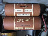 Two 8 μF, 525 V wound wet aluminum electrolytic capacitors in paper housing sealed with tar out of a 1930s radio.


Overlapping range of applications[edit | edit source]
These individual capacitors can perform their application independent of their affiliation to an above shown capacitor type, so that an overlapping range of applications between the different capacitor types exists.

Capacitor - types and styles[edit | edit source]
Ceramic capacitors[edit | edit source]

A ceramic capacitor is a non-polarized fixed capacitor made out of two or more alternating layers of ceramic and metal in which the ceramic material acts as the dielectric and the metal acts as the electrodes. The ceramic material is a mixture of finely ground granules of paraelectric or ferroelectric materials, modified by mixed oxides that are necessary to achieve the capacitor's desired characteristics. The electrical behavior of the ceramic material is divided into two stability classes:
- Class 1 ceramic capacitors with high stability and low losses compensating the influence of temperature in resonant circuit application. Common EIA/IEC code abbreviations are C0G/NP0, P2G/N150, R2G/N220, U2J/N750 etc.
- Class 2 ceramic capacitors with high volumetric efficiency for buffer, by-pass and coupling applications Common EIA/IEC code abbreviations are: X7R/2XI, Z5U/E26, Y5V/2F4, X7S/2C1, etc.
The great plasticity of ceramic raw material works well for many special applications and enables an enormous diversity of styles, shapes and great dimensional spread of ceramic capacitors. The smallest discrete capacitor, for instance, is a "01005" chip capacitor with the dimension of only 0.4 mm × 0.2 mm.
The construction of ceramic multilayer capacitors with mostly alternating layers results in single capacitors connected in parallel. This configuration increases capacitance and decreases all losses and parasitic inductances. Ceramic capacitors are well-suited for high frequencies and high current pulse loads.
Because the thickness of the ceramic dielectric layer can be easily controlled and produced by the desired application voltage, ceramic capacitors are available with rated voltages up to the 30 kV range.
Some ceramic capacitors of special shapes and styles are used as capacitors for special applications, including RFI/EMI suppression capacitors for connection to supply mains, also known as safety capacitors,[9][10] X2Y® capacitors for bypassing and decoupling applications,[11] feed-through capacitors for noise suppression by low-pass filters[12] and ceramic power capacitors for transmitters and HF applications.[13][14]
- Diverse styles of ceramic capacitors
-
 Multi-layer ceramic capacitors (MLCC chips) for SMD mounting
 -
 Ceramic X2Y® decoupling capacitors
 -
 Ceramic EMI suppression capacitors for connection to the supply mains (safety capacitor)
 -
 High voltage ceramic power capacitor


| Capacitor type | Dielectric | Features/applications | Disadvantages |
|---|---|---|---|
| Ceramic Class 1 capacitors | paraelectric ceramic mixture of Titanium dioxide modified by additives | Predictable linear and low capacitance change with operating temperature. Excellent high frequency characteristics with low losses. For temperature compensation in resonant circuit application. Available in voltages up to 15,000 V | Low permittivity ceramic, capacitors with low volumetric efficiency, larger dimensions than Class 2 capacitors |
| Ceramic Class 2 capacitors | ferroelectric ceramic mixture of barium titanate and suitable additives | High permittivity, high volumetric efficiency, smaller dimensions than Class 1 capacitors. For buffer, by-pass and coupling applications. Available in voltages up to 50,000 V. | Lower stability and higher losses than Class 1. Capacitance changes with change in applied voltage, with frequency and with aging effects. Slightly microphonic |
Film capacitors[edit | edit source]

Film capacitors or plastic film capacitors are non-polarized capacitors with an insulating plastic film as the dielectric. The dielectric films are drawn to a thin layer, provided with metallic electrodes and wound into a cylindrical winding. The electrodes of film capacitors may be metallized aluminum or zinc, applied on one or both sides of the plastic film, resulting in metallized film capacitors or a separate metallic foil overlying the film, called film/foil capacitors.
Metallized film capacitors offer self-healing properties. Dielectric breakdowns or shorts between the electrodes do not destroy the component. The metallized construction makes it possible to produce wound capacitors with larger capacitance values (up to 100 µF and larger) in smaller cases than within film/foil construction.
Film/foil capacitors or metal foil capacitors use two plastic films as the dielectric. Each film is covered with a thin metal foil, mostly aluminium, to form the electrodes. The advantage of this construction is the ease of connecting the metal foil electrodes, along with an excellent current pulse strength.
A key advantage of every film capacitor's internal construction is direct contact to the electrodes on both ends of the winding. This contact keeps all current paths very short. The design behaves like a large number of individual capacitors connected in parallel, thus reducing the internal ohmic losses (ESR) and parasitic inductance (ESL). The inherent geometry of film capacitor structure results in low ohmic losses and a low parasitic inductance, which makes them suitable for applications with high surge currents (snubbers) and for AC power applications, or for applications at higher frequencies.
The plastic films used as the dielectric for film capacitors are Polypropylene (PP), Polyester (PET), Polyphenylene sulfide (PPS), Polyethylene naphthalate (PEN), and Polytetrafluoroethylene or Teflon (PTFE). Polypropylene film material with a market share of something about 50% and Polyester film with something about 40% are the most used film materials. The rest of something about 10% will be used by all other materials including PPS and paper with roughly 3%, each.[15][16]
| Film material, abbreviated codes | |||||
|---|---|---|---|---|---|
| Film characteristics | PET | PEN | PPS | PP | |
| Relative permittivity at 1 kHz | 3.3 | 3.0 | 3.0 | 2.2 | |
| Minimum film thickness (µm) | 0.7–0.9 | 0.9–1.4 | 1.2 | 2.4–3.0 | |
| Moisture absorption (%) | low | 0.4 | 0.05 | <0.1 | |
| Dielectric strength (V/µm) | 580 | 500 | 470 | 650 | |
| Commercial realized voltage proof (V/µm) |
280 | 300 | 220 | 400 | |
| DC voltage range (V) | 50–1,000 | 16–250 | 16–100 | 40–2,000 | |
| Capacitance range | 100 pF–22 µF | 100 pF–1 µF | 100 pF–0.47 µF | 100 pF–10 µF | |
| Application temperature range (°C) | −55 to +125 /+150 | −55 to +150 | −55 to +150 | −55 to +105 | |
| ΔC/C versus temperature range (%) | ±5 | ±5 | ±1.5 | ±2.5 | |
| Dissipation factor (•10−4) | |||||
| at 1 kHz | 50–200 | 42–80 | 2–15 | 0.5–5 | |
| at 10 kHz | 110–150 | 54–150 | 2.5–25 | 2–8 | |
| at 100 kHz | 170–300 | 120–300 | 12–60 | 2–25 | |
| at 1 MHz | 200–350 | – | 18–70 | 4–40 | |
| Time constant RInsul•C (s) | at 25 °C | ≥10,000 | ≥10,000 | ≥10,000 | ≥100,000 |
| at 85 °C | 1,000 | 1,000 | 1,000 | 10,000 | |
| Dielectric absorption (%) | 0.2–0.5 | 1–1.2 | 0.05–0.1 | 0.01–0.1 | |
| Specific capacitance (nF•V/mm3) | 400 | 250 | 140 | 50 | |
Some film capacitors of special shapes and styles are used as capacitors for special applications, including RFI/EMI suppression capacitors for connection to the supply mains, also known as safety capacitors,[17] Snubber capacitors for very high surge currents,[18] Motor run capacitors, AC capacitors for motor-run applications[19]
- High pulse current load is the most important feature of film capacitors so many of the available styles do have special terminations for high currents
-
 Radial style (single ended) for through-hole solder mounting on printed circuit boards
 -
 SMD style for printed circuit board surface mounting, with metallized contacts on two opposite edges
 -
 Radial style with heavy-duty solder terminals for snubber applications and high surge pulse loads
 -
 Heavy-duty snubber capacitor with screw terminals


| Capacitor type | Dielectric | Features/applications | Disadvantages |
|---|---|---|---|
| Metallized film capacitors | PP, PET, PEN, PPS, (PTFE) | Metallized film capacitors are significantly smaller in size than film/foil versions and have self-healing properties. | Thin metallized electrodes limit the maximum current carrying capability respectively the maximum possible pulse voltage. |
| Film/foil film capacitors | PP, PET, PTFE | Film/foil film capacitors have the highest surge ratings/pulse voltage, respectively. Peak currents are higher than for metallized types. | No self-healing properties: internal short may be disabling. Larger dimensions than metallized alternative. |
| Polypropylene (PP) film capacitors | Polypropylene (Treofan®) |
Most popular film capacitor dielectric. Predictable linear and low capacitance change with operating temperature. Suitable for applications in Class-1 frequency-determining circuits and precision analog applications. Very narrow capacitances. Extremely low dissipation factor. Low moisture absorption, therefore suitable for "naked" designs with no coating. High insulation resistance. Usable in high power applications such as snubber or IGBT. Used also in AC power applications, such as in motors or power factor correction. Very low dielectric losses. High frequency and high power applications such as induction heating. Widely used for safety/EMI suppression, including connection to power supply mains. | Maximum operating temperature of 105 °C. Relatively low permittivity of 2.2. PP film capacitors tend to be larger than other film capacitors. More susceptible to damage from transient over-voltages or voltage reversals than oil-impregnated MKV-capacitors for pulsed power applications. |
| Polyester (PET) film (Mylar) capacitors |
Polyethylene terephthalate, Polyester (Hostaphan®, Mylar®) | Smaller in size than functionally comparable polypropylene film capacitors. Low moisture absorption. Have almost completely replaced metallized paper and polystyrene film for most DC applications. Mainly used for general purpose applications or semi-critical circuits with operating temperatures up to 125 °C. Operating voltages up to 60,000 V DC. | Usable at low (AC power) frequencies. Limited use in power electronics due to higher losses with increasing temperature and frequency. |
| Polyethylene naphthalate (PEN) film capacitors |
Polyethylene naphthalate (Kaladex®) | Better stability at high temperatures than PET. More suitable for high temperature applications and for SMD packaging. Mainly used for non-critical filtering, coupling and decoupling, because temperature dependencies are not significant. | Lower relative permittivity and lower dielectric strength imply larger dimensions for a given capacitance and rated voltage than PET. |
| Polyphenylene Sulfide (PPS) film capacitors |
Polyphenylene (Torelina®) | Small temperature dependence over the entire temperature range and a narrow frequency dependence in a wide frequency range. Dissipation factor is quite small and stable. Operating emperatures up to 270 °C. Suitable for SMD. Tolerate increased reflow soldering temperatures for lead-free soldering mandated by the RoHS 2002/95/European Union directive | Above 100 °C, the dissipation factor increases, increasing component temperature, but can operate without degradation. Cost is usually higher than PP. |
| Polytetrafluoroethylene (PTFE) (Teflon film) capacitors |
Polytetrafluoroethylene (Teflon®) | Lowest loss solid dielectric. Operating temperatures up to 250 °C. Extremely high insulation resistance. Good stability. Used in mission-critical applications. | Large size (due to low dielectric constant). Higher cost than other film capacitors. |
| Polycarbonate (PC) film capacitors |
Polycarbonate | Almost completely replaced by PP | Limited manufacturers |
| Polystyrene (PS) film capacitors |
Polystyrene (Styroflex) | Almost completely replaced by PET | Limited manufacturers |
| Polysulphone film capacitors | Polysulfone | Similar to polycarbonate. Withstand full voltage at comparatively higher temperatures. | Only development, no series found (2012) |
| Polyamide film capacitors | Polyamide | Operating temperatures of up to 200 °C. High insulation resistance. Good stability. Low dissipation factor. | Only development, no series found (2012) |
| Polyimide film (Kapton) capacitors |
Polyimide (Kapton) | Highest dielectric strength of any known plastic film dielectric. | Only development, no series found (2012) |
Film power capacitors[edit | edit source]

A related type is the power film capacitor. The materials and construction techniques used for large power film capacitors mostly are similar to those of ordinary film capacitors. However, capacitors with high to very high power ratings for applications in power systems and electrical installations are often classified separately, for historical reasons. The standardization of ordinary film capacitors is oriented on electrical and mechanical parameters. The standardization of power capacitors by contrast emphasizes the safety of personnel and equipment, as given by the local regulating authority.
As modern electronic equipment gained the capacity to handle power levels that were previously the exclusive domain of "electrical power" components, the distinction between the "electronic" and "electrical" power ratings blurred. Historically, the boundary between these two families was approximately at a reactive power of 200 volt-amps.
Film power capacitors mostly use polypropylene film as the dielectric. Other types include metallized paper capacitors (MP capacitors) and mixed dielectric film capacitors with polypropylene dielectrics. MP capacitors serve for cost applications and as field-free carrier electrodes (soggy foil capacitors) for high AC or high current pulse loads. Windings can be filled with an insulating oil or with epoxy resin to reduce air bubbles, thereby preventing short circuits.
They find use as converters to change voltage, current or frequency, to store or deliver abruptly electric energy or to improve the power factor. The rated voltage range of these capacitors is from approximately120 V AC (capacitive lighting ballasts) to 100 kV.[20]
- Power film capacitors for applications in power systems, electrical installations and plants
-
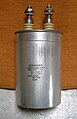 Power film capacitor for AC Power factor correction (PFC), packaged in a cylindrical metal can
 -
 Power film capacitor in rectangular housing
 -

-
 75MVAR substation capacitor bank at 150kV


| Capacitor type | Dielectric | Features/applications | Disadvantages |
|---|---|---|---|
| Metallized paper power capacitors | Paper impregnated with insulating oil or epoxy resin | Self-healing properties. Originally impregnated with wax, oil or epoxy. Oil-Kraft paper version used in certain high voltage applications. Mostly replaced by PP. | Large size. Highly hygroscopic, absorbing moisture from the atmosphere despite plastic enclosures and impregnates. Moisture increases dielectric losses and decreases insulation resistance. |
| Paper film/foil power capacitors | Kraft paper impregnated with oil | Paper covered with metal foils as electrodes. Low cost. Intermittent duty, high discharge applications. | Physically large and heavy. Significantly lower energy density than PP dielectric. Not self-healing. Potential catastrophic failure due to high stored energy. |
| PP dielectric, field-free paper power capacitors (MKV power capacitors) |
Double-sided (field-free) metallized paper as electrode carrier. PP as dielectic, impregnated with insulating oil, epoxy resin or insulating gas | Self-healing. Very low losses. High insulation resistance. High inrush current strength. High thermal stability. Heavy duty applications such as commutating with high reactive power, high frequencies and a high peak current load and other AC applications. | Physically larger than PP power capacitors. |
| Single- or double-sided metallized PP power capacitors |
PP as dielectric, impregnated with insulating oil, epoxy resin or insulating gas | Highest capacitance per volume power capacitor. Self-healing. Broad range of applications such as general-purpose, AC capacitors, motor capacitors, smoothing or filtering, DC links, snubbing or clamping, damping AC, series resonant DC circuits, DC discharge, AC commutation, AC power factor correction. | critical for reliable high voltage operation and very high inrush current loads, limited heat resistance (105 °C) |
| PP film/foil power capacitors | Impregnated PP or insulating gas, insulating oil, epoxy resin or insulating gas | Highest inrush current strength | Larger than the PP metallized versions. Not self-healing. |
Electrolytic capacitors[edit | edit source]
Electrolytic capacitors have a metallic anode covered with an oxidized layer used as dielectric. The second electrode is a non-solid (wet) or solid electrolyte. Electrolytic capacitors are polarized. Three families are available, categorized according to their dielectric.
- Aluminum electrolytic capacitors with aluminum oxide as dielectric
- Tantalum electrolytic capacitors with tantalum pentoxide as dielectric
- Niobium electrolytic capacitors with niobium pentoxide as dielectric.
The anode is highly roughened to increase the surface area. This and the relatively high permittivity of the oxide layer gives these capacitors very high capacitance per unit volume compared with film- or ceramic capacitors.
The permittivity of tantalum pentoxide is approximately three times higher than aluminium dioxide, producing significantly smaller components. However, permittivity determines only the dimensions. Electrical parameters, especially conductivity, are established by the electrolyte's material and composition. Three general types of electrolytes are used:
- non solid (wet, liquid)—conductivity approximately 10 mS/cm and are the lowest cost
- solid manganese oxide—conductivity approximately 100 mS/cm offer high quality and stability
- solid conductive polymer (Polypyrrole)—conductivity approximately 10,000 mS/cm,[21] offer ESR values as low as <10 mΩ
Internal losses of electrolytic capacitors, prevailing used for decoupling and buffering applications, are determined by the kind of electrolyte.
| Anode material | Electrolyte | Capacitance range (µF) |
Max. rated voltage at 85 °C (V) |
Upper categorie temperature (°C) |
Specific ripple current (mA/mm3) 1) |
|---|---|---|---|---|---|
| Aluminum (roughned foil) |
non solid, e.g. Ethylene glycol, DMF, DMA, GBL |
0.1–2,700,000 | 600 | 150 | 0.05–2.0 |
| solid, Manganese dioxide (MnO2 |
0.1–1,500 | 40 | 175 | 0.5–2.5 | |
| solid conductive polymere (e.g. Polypyrrole) |
10–1,500 | 25 | 125 | 10–30 | |
| Tantalum (roughned foil) |
non solid Sulfuric acid |
0.1–1,000 | 630 | 125 | – |
| Tantalum (sintered) |
non solid sulfuric acid |
0.1–15,000 | 150 | 200 | – |
| solid Manganese dioxide (MnO2 |
0.1–3,300 | 125 | 150 | 1.5–15 | |
| solid conductive polymere (e.g. Polypyrrole) |
10–1,500 | 35 | 125 | 10–30 | |
| Niobium (sintered) |
solid Manganese dioxide (MnO2 |
1–1,500 | 10 | 125 | 5–20 |
| solid conductive polymere (e.g. Polypyrrole) |
2.2–1,000 | 25 | 105 | 10–30 | |
| |||||
The large capacitance per unit volume of electrolytic capacitors make them valuable in relatively high-current and low-frequency electrical circuits, e.g. in power supply filters for decoupling unwanted AC components from DC power connections or as coupling capacitors in audio amplifiers, for passing or bypassing low-frequency signals and storing large amounts of energy. The relatively high capacitance value of an electrolytic capacitor combined with the very low ESR of the polymer electrolyte of polymer capacitors, especially in SMD styles, makes them a competitor to MLC chip capacitors in personal computer power supplies.
Bipolar electrolytics (also called Non-Polarized capacitors) contain two anodized aluminium foils, behaving like two capacitors connected in series opposition.
Electolytic capacitors for special applications include motor start capacitors,[22] flashlight capacitors[23] and audio frequency capacitors.[24]
- Schematic representation
-
 Schematic representation of the structure of a wound aluminum electrolytic capacitor with non solid (liquid) electrolyte
 -
 Schematic representation of the structure of a sintered tantalum electrolytic capacitor with solid electrolyte


- Aluminum, tantalum and niobium electrolytic capacitors
-
 Axial, radial (single ended) anv V-chip styles of aluminum electrolytic capacitors
 -
 Snap-in style of aluminum electrolytic capacitors for power applications
 -
 SMD style for surface mounting of aluminum electrolytic capacitors with polymer electrolyte
 -
 Tantalum electrolytic chip capacitors for surface mounting


| Capacitor type | Dielectric | Features/applications | Disadvantages |
|---|---|---|---|
| Electrolytic capacitors with non solid (wet, liquid) electrolyte |
Aluminum dioxide Al2O3 |
Very large capacitance to volume ratio. Capacitance values up to 2,700,000 µF/6.3 V. Voltage up to 550 V. Lowest cost per capacitance/voltage values. Used where low losses and high capacitance stability are not of major importance, especially for lower frequencies, such as by-pass, coupling, smoothing and buffer applications in power supplies and DC-links. | Polarized. Significant leakage. Relatively high ESRTemplate:Dn and ESL values, limiting high ripple current and high frequency applications. Lifetime calculation required because drying out phenomenon. Vent or burst when overloaded, overheated or connected wrong polarized. Water based electrolyte may vent at end-of-life, showing failures like "capacitor plague" |
| Tantalum pentoxide Ta2O5 |
Wet tantalum electrolytic capacitors (wet slug)[25] Lowest leakage among electrolytics. Voltage up to 630 V (tantalum film) or 125 V (tantalum sinter body). Hermetically sealed. Stable and reliable. Military and space applications. | Polarized. Violent explosion when voltage, ripple current or slew rates are exceeded, or under reverse voltage. Expensive. | |
| [Electrolytic capacitors with solid [Manganese dioxide]] electrolyte |
Aluminum dioxide Al2O3 Tantalum pentoxide Ta2O5, Niobium pentoxide Nb2O5 |
Tantalum and niobium with smaller dimensions for a given capacitance/voltage vs aluminum. Stable electrical parameters. Good long-term high temperature performance. Lower ESR lower than non-solid (wet) electrolytics. | Polarized. About 125 V. Low voltage and limited, transient, reverse or surge voltage tolerance. Possible combustion upon failure. ESR much higher than conductive polymer electrolytics. Manganese expected to be replaced by polymer. |
| Electrolytic capacitors with solid Polymer electrolyte (Polymer capacitors) |
Aluminum dioxide Al2O3, Tantalum pentoxide Ta2O5, Niobium pentoxide Nb2O5 |
Greatly reduced ESR compared with manganese or non-solid (wet) elelectrolytics. Higher ripple current ratings. Extended operational life. Stable electrical parameters. Self-healing.[26] Used for smoothing and buffering in smaller power supplies especially in SMD. | Polarized. Highest leakage current among electrolytics. Higher prices than non-solid or manganese dioxide. Voltage limited to about 100 V. Explodes when voltage, current, or slew rates are exceeded or under reverse voltage. |
Supercapacitors[edit | edit source]


Supercapacitors (SC),[27] comprise a family of electrochemical capacitors. Supercapacitor, sometimes called ultracapacitor is a generic term for electric double-layer capacitors (EDLC), pseudocapacitors and hybrid capacitors. They don't have a conventional solid dielectric. The capacitance value of an electrochemical capacitor is determined by two storage principles, both of which contribute to the total capacitance of the capacitor:[28][29][30]
- Double-layer capacitance – Storage is achieved by separation of charge in a Helmholtz double layer at the interface between the surface of a conductor and an electrolytic solution. The distance of separation of charge in a double-layer is on the order of a few Angstroms (0.3–0.8 nm). This storage is electrostatic in origin.[2]
- Pseudocapacitance – Storage is achieved by redox reactions, electrosorbtion or intercalation on the surface of the electrode or by specifically adsorpted ions that results in a reversible faradaic charge-transfer. The pseudocapacitance is faradaic in origin.[2]
The ratio of the storage resulting from each principle can vary greatly, depending on electrode design and electrolyte composition. Pseudocapacitance can increase the capacitance value by as much as an order of magnitude over that of the double-layer by itself.[27]
Supercapacitors are divided into three families, based on the design of the electrodes:
- Double-layer capacitors – with carbon electrodes or derivates with much higher static double-layer capacitance than the faradaic pseudocapacitance
- Pseudocapacitors – with electrodes out of metal oxides or conducting polymers with a high amount of faradaic pseudocapacitance
- Hybrid capacitors – capacitors with special and asymmetric electrodes that exhibit both significant double-layer capacitance and pseudocapacitance, such as lithium-ion capacitors
Supercapacitors bridge the gap between conventional capacitors and rechargeable batteries. They have the highest available capacitance values per unit volume and the greatest energy density of all capacitors. They support up to 12,000 Farads/1.2 Volt,[31] with capacitance values up to 10,000 times that of electrolytic capacitors.[27] While existing supercapacitors have energy densities that are approximately 10% of a conventional battery, their power density is generally 10 to 100 times greater. Power density is defined as the product of energy density, multiplied by the speed at which the energy is delivered to the load. The greater power density results in much shorter charge/discharge cycles than a battery is capable, and a greater tolerance for numerous charge/discharge cycles. This makes them well-suited for parallel connection with batteries, and may improve battery performance in terms of power density.
Within electrochemical capacitors, the electrolyte is the conductive connection between the two electrodes, distinguishing them from electrolytic capacitors, in which the electrolyte only forms the cathode, the second electrode.
Supercapacitors are polarized and must operate with correct polarity. Polarity is controlled by design with asymmetric electrodes, or, for symmetric electrodes, by a potential applied during the manufacturing process.
Supercapacitors support a broad spectrum of applications for power and energy requirements, including:
- Low supply current during longer times for memory backup in (SRAMs) in electronic equipment
- Power electronics that require very short, high current, as in the KERSsystem in Formula 1 cars
- Recovery of braking energy for vehicles such as buses and trains
Supercapacitors are rarely interchangeable, especially those with higher energy densities. IEC standard 62391-1 Fixed electric double layer capacitors for use in electronic equipment identifies four application classes:
- Class 1, Memory backup, discharge current in mA = 1 • C (F)
- Class 2, Energy storage, discharge current in mA = 0.4 • C (F) • V (V)
- Class 3, Power, discharge current in mA = 4 • C (F) • V (V)
- Class 4, Instantaneous power, discharge current in mA = 40 • C (F) • V (V)
Exceptional for electronic components like capacitors are the manifold different trade or series names used for supercapacitors like: APowerCap, BestCap, BoostCap, CAP-XX, DLCAP, EneCapTen, EVerCAP, DynaCap, Faradcap, GreenCap, Goldcap, HY-CAP, Kapton capacitor, Super capacitor, SuperCap, PAS Capacitor, PowerStor, PseudoCap, Ultracapacitor making it difficult for users to classify these capacitors.
- Double-layer, Lithium-Ion and supercapacitors
-
 Double-layer capacitor with 1 F at 5.5 V for data buffering
 -
 Radial (single ended) style of lithium ion capacitors for high energy density
 -
Supercapacitor/Ultracapacitor cells and modules for high current loads


| Capacitor type | Dielectric | Features/applications | Disadvantages |
|---|---|---|---|
| Supercapacitors Pseudocapacitors |
Helmholtz double-layer plus faradaic pseudo-capacitance | Energy density typically tens to hundreds of times greater than conventional electrolytics. More comparable to batteries than to other capacitors. Large capacitance/volume ratio. Relatively low ESR. Thousands of farads. RAM memory backup. Temporary power during battery replacement. Rapidly absorbs/delivers much larger currents than batteries. Hundreds of thousands of charge/discharge cycles. Hybrid vehicles. Recuperation | Polarized. Low operating voltage per cell. (Stacked cells provide higher operating voltage.) Relatively high cost. |
| Hybrid capacitors Lithium ion capacitors (LIC) |
Helmholtz double-layer plus faradaic pseudo-capacitance. Anode doped with lithium ions. | Higher operating voltage. Higher energy density than common EDLCs, but smaller than lithium ion batteries (LIB). No thermal runaway reactions. | Polarized. Low operating voltage per cell. (Stacked cells provide higher operating voltage.) Relatively high cost. |
Miscellaneous capacitors[edit | edit source]
Beneath the above described capacitors covering more or less nearly the total market of discrete capacitors some new developments or very special capacitor types as well as older types can be found in electronics.
Integrated capacitors[edit | edit source]
- Integrated capacitors—in integrated circuits, nano-scale capacitors can be formed by appropriate patterns of metallization on an isolating substrate. They may be packaged in multiple capacitor arrays with no other semiconductive parts as discrete components.[32]
- Glass capacitors—First Leyden jar capacitor was made of glass, As of 2012[update] glass capacitors were in use as SMD version for applications requiring ultra-reliable and ultra-stable service.
Power capacitors[edit | edit source]
- Vacuum capacitors—used in high power RF transmitters
- SF6 gas filled capacitors—used as capacitance standard in measuring bridge circuits
Special capacitors[edit | edit source]
- Printed circuit boards—metal conductive areas in different layers of a multi-layer printed circuit board can act as a highly stable capacitor. It is common industry practice to fill unused areas of one PCB layer with the ground conductor and another layer with the power conductor, forming a large distributed capacitor between the layers.
- Wire—2 pieces of insulated wire twisted together. Capacitance alues usually range from 3 pF to 15 pF. Used in homemade VHF circuits for oscillation feedback.
Obsolete capacitors[edit | edit source]
- Mica capacitors—the first capacitors with stable frequency behavior and low losses, used for military radio applications during World War II
- Air-gap capacitors—used by the first spark-gap transmitters
- Miscellaneous capacitors
-
 Some 1nF × 500VDC rated silver mica capacitors
 -
 Vacuum capacitor with uranium glass encapsulation


| Capacitor type | Dielectric | Features/applications | Disadvantages |
|---|---|---|---|
| Air gap capacitors | Air | Low dielectric loss. Used for resonating HF circuits for high power HF welding. | Physically large. Relatively low capacitance. |
| Vacuum capacitors | Vacuum | Extremely low losses. Used for high voltage, high power RF applications, such as transmitters and induction heating. Self-healing if arc-over current is limited. | Very high cost. Fragile. Large. Relatively low capacitance. |
| SF6-gas filled capacitors | SF6 gas | High precision.[33] Extremely low losses. Very high stability. Up to 1600 kV rated voltage. Used as capacitance standard in measuring bridge circuits. | Very high cost |
| Metallized mica (Silver mica) capacitors | Mica | Very high stability. No aging. Low losses. Used for HF and low VHF RF circuits and as capacitance standard in measuring bridge circuits. Mostly replaced by Class 1 ceramic capacitors | Higher cost than class 1 ceramic capacitors |
| Glass capacitors | Glass | Better stability and frequency than silver mica. Ultra-reliable. Ultra-stable. Resistant to nuclear radiation. Operating temperature: −75 °C to +200 °C and even short overexposure to +250 °C.[34] | Higher cost than class 1 ceramic |
| Integrated capacitors | oxide-nitride-oxide (ONO) | Thin (down to 100 µm). Smaller footprint than most MLCC. Low ESL. Very high stability up to 200 °C. High reliability | Customized production |
Variable capacitors[edit | edit source]
Variable capacitors may have their capacitance changed by mechanical motion. Generally two versions of variable capacitors has to be to distinguished
- Tuning capacitor – variable capacitor for intentionally and repeatedly tuning an oscillator circuit in a radio or another tuned circuit
- Trimmer capacitor – small variable capacitor usually for one-time oscillator circuit internal adjustment
Variable capacitors include capacitors that use a mechanical construction to change the distance between the plates, or the amount of plate surface area which overlaps. They mostly use air as dielectric medium.
Semiconductive variable capacitance diodes are not capacitors in the sense of passive components but can change their capacitance as a function of the applied reverse bias voltage and are used like a variable capacitor. They have replaced much of the tuning and trimmer capacitors.
- Variable capacitors
-
 Air gap tuning capacitor
 -
 Vacuum tuning capacitor
 -
 Trimmer capacitor for through hole mounting
 -
 Trimmer capacitor for surface mounting


| Capacitor type | Dielectric | Features/applications | Disadvantages |
|---|---|---|---|
| Air gap tuning capacitors | Air | Circular or various logarithmic cuts of the rotor electrode for different capacitance curves. Split rotor or stator cut for symmetric adjustment. Ball bearing axis for noise reduced adjustment. For high professional devices. | Large dimensions. High cost. |
| Vacuum tuning capacitors | Vacuum | Extremely low losses. Used for high voltage, high power RF applications, such as transmitters and induction heating. Self-healing if arc-over current is limited. | Very high cost. Fragile. Large dimensions. |
| SF6 gas filled tuning capacitor | SF6 | Extremely low losses. Used for very high voltage high power RF applications. | Very high cost, fragile, large dimensions |
| Air gap trimmer capacitors | Air | Mostly replaced by semiconductive variable capacitance diodes | High cost |
| Ceramic trimmer capacitors | Class 1 ceramic | Linear and stable frequency behavior over wide temperature range | High cost |
Market[edit | edit source]
Discrete capacitors today are industrial products produced in very large quantities for use in electronic and in electrical equipment. Globally, the market for fixed capacitors was estimated at approximately US$18 billion in 2008 for 1,400 billion (1.4 × 10¹²) pieces.[35] This market is dominated by ceramic capacitors with estimate of approximately one trillion (1 × 10¹²) items per year.[1]
Detailed estimated figures in value for the main capacitor families are:
- Ceramic capacitors—US$8.3 billion (46%);
- Aluminum electrolytic capacitors—US$ 3.9 billion (22%);
- Film capacitors and Paper capacitors—US$ 2.6 billion, (15%);
- Tantalum electrolytic capacitors—US$ 2.2 billion (12%);
- Super capacitors (Double-layer capacitors)—US$ 0.3 billion (2%); and
- Others like silver mica and vacuum capacitors—US$ 0.7 billion (3%).
All other capacitor types are negligible in terms of value and quantity compared with the above types.
Capacitor - Electrical characteristics[edit | edit source]
Series-equivalent circuit[edit | edit source]

Discrete capacitors deviate from the ideal capacitor. An ideal capacitor only stores and releases electrical energy, with no dissipation. Capacitor components have losses and parasitic inductive parts. These imperfections in material and construction can have positive implications such as linear frequency and temperature behavior in class 1 ceramic capacitors. Conversely, negative implications include the non-linear, voltage-dependent capacitance in class 2 ceramic capacitors or the insufficient dielectric insulation of capacitors leading to leakage currents.
All properties can be defined and specified by a series equivalent circuit composed out of an idealized capacitance and additional electrical components which model all losses and inductive parameters of a capacitor. In this series-equivalent circuit the electrical characteristics are defined by:
- C, the capacitance of the capacitor
- Rinsul, the insulation resistance of the dielectric, not to be confused with the insulation of the housing
- Rleak, the resistance representing the leakage current of the capacitor
- RESR, the equivalent series resistance which summarizes all ohmic losses of the capacitor, usually abbreviated as "ESR"
- LESL, the equivalent series inductance which is the effective self-inductance of the capacitor, usually abbreviated as "ESL".
Using a series equivalent circuit instead of a parallel equivalent circuit is specified by IEC/EN 60384-1.
Standard values and tolerances[edit | edit source]
The "rated capacitance" CR or "nominal capacitance" CN is the value for which the capacitor has been designed. Actual capacitance depends on the measured frequency and ambient temperature. Standard measuring conditions are a low-voltage AC measuring method at a temperature of 20 °C with frequencies of
- 100 kHz, 1 MHz (preferred) or 10 MHz for non-electrolytic capacitors with CR ≤ 1 nF:
- 1 kHz or 10 kHz for non-electrolytic capacitors with 1 nF < CR ≤ 10 μF
- 100/120 Hz for electrolytic capacitors
- 50/60 Hz or 100/120 Hz for non-electrolytic capacitors with CR > 10 μF
For supercapacitors a voltage drop method is applied for measuring the capacitance value. .
Capacitors are available in geometrically increasing preferred values (E series standards) specified in IEC/EN 60063. According to the number of values per decade, these were called the E3, E6, E12, E24 etc. series. The range of units used to specify capacitor values has expanded to include everything from pico- (pF), nano- (nF) and microfarad (µF) to farad (F). Millifarad and kilofarad are uncommon.
The percentage of allowed deviation from the rated value is called tolerance. The actual capacitance value should be within its tolerance limits, or it is out of specification. IEC/EN 60062 specifies a letter code for each tolerance.
| E series | Tolerance | |||
|---|---|---|---|---|
| CR > 10 pF | Letter code | CR < 10 pF | Letter code | |
| E 96 | 1% | F | 0.1 pF | B |
| E 48 | 2% | G | 0.25 pF | C |
| E 24 | 5% | J | 0.5 pF | D |
| E 12 | 10% | K | 1 pF | F |
| E 6 | 20% | M | 2 pF | G |
| E3 | −20/+50% | S | - | - |
| −20/+80% | Z | - | - | |
The required tolerance is determined by the particular application. The narrow tolerances of E24 to E96 are used for high-quality circuits such as precision oscillators and timers. General applications such as non-critical filtering or coupling circuits employ E12 or E6. Electrolytic capacitors, which are often used for filtering and bypassing capacitors mostly have a tolerance range of ±20% and need to conform to E6 (or E3) series values.
Temperature dependence[edit | edit source]
Capacitance typically varies with temperature. The different dielectrics express great differences in temperature sensitivity. The temperature coefficient is expressed in parts per million (ppm) per degree Celsius for class 1 ceramic capacitors or in % over the total temperature range for all others.
| Type of capacitor, dielectric material |
Temperature coefficient ΔC/C |
Application temperature range |
|---|---|---|
| Ceramic capacitor class 1 paraelectric NP0 |
± 30 ppm/K (±0.5 %) | −55 to +125 °C |
| Ceramic capacitor class 2 ferroelectric X7R |
±15 % | −55 to +125 °C |
| Ceramic capacitor class 2, ferroelectric Y5V |
+22 % / −82 % | −30 to +85 °C |
| Film capacitor Polypropylene ( PP) |
±2.5 % | −55 to +85/105 °C |
| Film capacitor Polyethylen terephthalate, Polyester (PET) |
+5 % | −55 to +125/150 °C |
| Film capacitor Polyphenylene sulfide (PPS) |
±1.5 % | −55 to +150 °C |
| Film capacitor Polyethylene naphthalate (PEN) |
±5 % | −40 to +125/150 °C |
| Film capacitor Polytetrafluoroethylene (PTFE) |
? | −40 to +130 °C |
| Metallized paper capacitor (impregnated) | ±10 % | −25 to +85 °C |
| Aluminum electrolytic capacitor Al2O3 |
±20 % | −40 to +85/105/125 °C |
| Tantalum electrolytic capacitor Ta2O5 |
±20 % | −40 to +125 °C |
Frequency dependence[edit | edit source]
Most discrete capacitor types have more or less capacitance changes with increasing frequencies. The dielectric strength of class 2 ceramic and plastic film diminishes with rising frequency. Therefore their capacitance value decreases with increasing frequency. This phenomenon for ceramic class 2 and plastic film dielectrics is related to dielectric relaxation in which the time constant of the electrical dipoles is the reason for the frequency dependence of permittivity. The graphs below show typical frequency behavior of the capacitance for ceramic and film capacitors.
- Frequency dependence of capacitance for ceramic and film capacitors
-
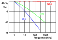 Frequency dependence of capacitance for ceramic class 2 capacitors (NP0 class 1 for comparisation)
 -
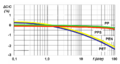 Frequency dependence of capacitance for film capacitors with different film materials


For electrolytic capacitors with non-solid electrolyte, mechanical motion of the ions occurs. Their movability is limited so that at higher frequencies not all areas of the roughened anode structure are covered with charge-carrying ions. As higher the anode structure is roughned as more the capacitance value decreases with increasing frequency. Low voltage types with highly-roughened anodes display capacitance at 100 kHz approximately 10 to 20% of the value measured at 100 Hz.
Voltage dependence[edit | edit source]
Capacitance may also change with applied voltage. This effect is more prevalent in class 2 ceramic capacitors. The permittivity of ferroelectric class 2 material depends on the applied voltage. Higher applied voltage lowers permittivity. The change of capacitance can drop to 80% of the value measured with the standardized measuring voltage of 0.5 or 1.0 V. This behavior is a small source of non-linearity in low-distortion filters and other analog applications. In audio applications this can be the reason for harmonic distortion.
Film capacitors and electrolytic capacitors have no significant voltage dependence.
- Voltage dependence of capacitance for some different class 2 ceramic capacitors
-
 Simplified diagram of the change in capacitance as a function of the applied voltage for 25-V capacitors in different kind of ceramic grades
 -
 Simplified diagram of the change in capacitance as a function of applied voltage for X7R ceramics with different rated voltages


Rated and category voltage[edit | edit source]

The voltage at which the dielectric becomes conductive is called the breakdown voltage, and is given by the product of the dielectric strength and the separation between the electrodes. The dielectric strength depends on temperature, frequency, shape of the electrodes, etc. Because a breakdown in a capacitor normally is a short circuit and destroys the component, the operating voltage is lower than the breakdown voltage. The operating voltage is specified such that the voltage may be applied continuously throughout the life of the capacitor.
In IEC/EN 60384-1 the allowed operating voltage is called "rated voltage" or "nominal voltage". The rated voltage (UR) is the maximum DC voltage or peak pulse voltage that may be applied continuously at any temperature within the rated temperature range.
The voltage proof of nearly all capacitors decreases with increasing temperature. For some applications it is important to use a higher temperature range. Lowering the voltage applied at a higher temperature maintains safety margins. For some capacitor types therefore the IEC standard specify a second "temperature derated voltage" for a higher temperature range, the "category voltage". The category voltage (UC) is the maximum DC voltage or peak pulse voltage that may be applied continuously to a capacitor at any temperature within the category temperature range.
The relation between both voltages and temperatures is given in the picture right.
Impedance[edit | edit source]

In general, a capacitor is seen as a storage component for electric energy. But this is only one capacitor function. A capacitor can also act as an AC resistor. In many cases the capacitor is used as a decoupling capacitor to filter or bypass undesired biased AC frequencies to the ground. Other applications use capacitors for capacitive coupling of AC signals; the dielectric is used only for blocking DC. For such applications the AC resistance is as important as the capacitance value.
The frequency dependent AC resistance is called impedance and is the complex ratio of the voltage to the current in an AC circuit. Impedance extends the concept of resistance to AC circuits and possesses both magnitude and phase at a particular frequency. This is unlike resistance, which has only magnitude.


The magnitude represents the ratio of the voltage difference amplitude to the current amplitude, is the imaginary unit, while the argument gives the phase difference between voltage and current.


In capacitor data sheets, only the impedance magnitude |Z| is specified, and simply written as "Z" so that the formula for the impedance can be written in Cartesian form

where the real part of impedance is the resistance (for capacitors ) and the imaginary part is the reactance .


As shown in a capacitor's series-equivalent circuit, the real component includes an ideal capacitor , an inductance and a resistor . The total reactance at the angular frequency therefore is given by the geometric (complex) addition of a capacitive reactance (Capacitance) and an inductive reactance (Inductance): .


To calculate the impedance the resistance has to be added geometrically and then is given by

- . The impedance is a measure of the capacitor's ability to pass alternating currents. In this sense the impedance can be used like Ohms law


to calculate either the peak or the effective value of the current or the voltage.
In the special case of resonance, in which the both reactive resistances
- and
have the same value (), then the impedance will only be determined by .


The impedance specified in the datasheets often show typical curves for the different capacitance values. With increasing frequency as the impedance decreases down to a minimum. The lower the impedance, the more easily alternating currents can be passed through the capacitor. At the apex, the point of resonance, where XC has the same value than XL, the capacitor has the lowest impedance value. Here only the ESR determines the impedance. With frequencies above the resonance the impedance increases again due to the ESL of the capacitor. The capacitor becomes to an inductance.
As shown in the graph, the higher capacitance values can fit the lower frequencies better while the lower capacitance values can fit better the higher frequencies.
Aluminum electrolytic capacitors have relatively good decoupling properties in the lower frequency range up to about 1 MHz due to their large capacitance values. This is the reason for using electrolytic capacitors in standard or switched-mode power supplies behind the rectifier for smoothing application.
Ceramic and film capacitors are already out of their smaller capacitance values suitable for higher frequencies up to several 100 MHz. They also have significantly lower parasitic inductance, making them suitable for higher frequency applications, due to their construction with end-surface contacting of the electrodes. To increase the range of frequencies, often an electrolytic capacitor is connected in parallel with a ceramic or film capacitor.[36]
Many new developments are targeted at reducing parasitic inductance (ESL). This increases the resonance frequency of the capacitor and, for example, can follow the constantly increasing switching speed of digital circuits. Miniaturization, especially in the SMD multilayer ceramic chip capacitors (MLCC), increases the resonance frequency. Parasitic inductance is further lowered by placing the electrodes on the longitudinal side of the chip instead of the lateral side. The "face-down" construction associated with multi-anode technology in tantalum electrolytic capacitors further reduced ESL. Capacitor families such as the so-called MOS capacitor or silicon capacitors offer solutions when capacitors at frequencies up to the GHz range are needed.
Inductance (ESL) and self-resonant frequency[edit | edit source]
ESL in industrial capacitors is mainly caused by the leads and internal connections used to connect the capacitor plates to the outside world. Large capacitors tend to have higher ESL than small ones because the distances to the plate are longer and every mm counts as an inductance.
For any discrete capacitor, there is a frequency above DC at which it ceases to behave as a pure capacitor. This frequency, where is as high as , is called the self-resonant frequency. The self-resonant frequency is the lowest frequency at which the impedance passes through a minimum. For any AC application the self-resonant frequency is the highest frequency at which capacitors can be used as a capacitive component.


This is critically important for decoupling high-speed logic circuits from the power supply. The decoupling capacitor supplies transient current to the chip. Without decouplers, the IC demands current faster than the connection to the power supply can supply it, as parts of the circuit rapidly switch on and off. To counter this potential problem, circuits frequently use multiple bypass capacitors—small (100 nF or less) capacitors rated for high frequencies, a large electrolytic capacitor rated for lower frequencies and occasionally, an intermediate value capacitor.
Ohmic losses, ESR, dissipation factor, and quality factor[edit | edit source]
The summarized losses in discrete capacitors are ohmic AC losses. DC losses are specified as "leakage current" or "insulating resistance" and are negligible for an AC specification. AC losses are non-linear, possibly depending on frequency, temperature, age or humidity. The losses result from two physical conditions:
- line losses including internal supply line resistances, the contact resistance of the electrode contact, line resistance of the electrodes, and in "wet" aluminum electrolytic capacitors and especially supercapacitors, the limited conductivity of liquid electrolytes and
- dielectric losses from dielectric polarization.
The largest share of these losses in larger capacitors is usually the frequency dependent ohmic dielectric losses. For smaller components, especially for wet electrolytic capacitors, conductivity of liquid electrolytes may exceed dielectric losses. To measure these losses, the measurement frequency must be set. Since commercially available components offer capacitance values cover 15 orders of magnitude, ranging from pF (10−12 F) to some 1000 F in supercapacitors, it is not possible to capture the entire range with only one frequency. IEC 60384-1 states that ohmic losses should be measured at the same frequency used to measure capacitance. These are:
- 100 kHz, 1 MHz (preferred) or 10 MHz for non-electrolytic capacitors with CR ≤ 1 nF:
- 1 kHz or 10 kHz for non-electrolytic capacitors with 1 nF < CR ≤ 10 μF
- 100/120 Hz for electrolytic capacitors
- 50/60 Hz or 100/120 Hz for non-electrolytic capacitors with CR > 10 μF
A capacitor's summarized resistive losses may be specified either as ESR, as a dissipation factor(DF, tan δ), or as quality factor (Q), depending on application requirements.
Capacitors with higher ripple current loads, such as electrolytic capacitors, are specified with equivalent series resistance ESR. ESR can be shown as an ohmic part in the above vector diagram. ESR values are specified in datasheets per individual type.

The losses of film capacitors and some class 2 ceramic capacitors are mostly specified with the dissipation factor tan δ. These capacitors have smaller losses than electrolytic capacitors and mostly are used at higher frequencies up to some hundred MHz. However the numeric value of the dissipation factor, measured at the same frequency, is independent on the capacitance value and can be specified for a capacitor series with a range of capacitance. The dissipation factor is determined as the tangent of the reactance () and the ESR, and can be shown as the angle δ between imaginary and the impedance axis.

If the inductance is small, the dissipation factor can be approximated as:


Capacitors with very low losses, such as ceramic Class 1 and Class 2 capacitors, specify resistive losses with a quality factor (Q). Ceramic Class 1 capacitors are especially suitable for LC resonant circuits with frequencies up to the GHz range, and precise high and low pass filters. For an electrically resonant system, Q represents the effect of electrical resistance and characterizes a resonator's bandwidth relative to its center or resonant frequency . Q is defined as the reciprocal value of the dissipation factor.


A high Q value is for resonant circuits a mark of the quality of the resonance.
| Capacitor type | Capacitance (pF) |
ESR at 100 kHz (mΩ) |
ESR at 1 MHz (mΩ) |
tan δ at 1 MHz (10−4) |
Quality factor |
|---|---|---|---|---|---|
| Silicon capacitor[37] | 560 | 400 | — | 2,5 | 4000 |
| Mica capacitor[38] | 1000 | 650 | 65 | 4 | 2500 |
| Class 1 ceramic capacitor (NP0)[39] |
1000 | 1600 | 160 | 10 | 1000 |
Limiting current loads[edit | edit source]
A capacitor can act as an AC resistor, coupling AC voltage and AC current between two points. Every AC current flow through a capacitor generates heat inside the capacitor body. These dissipation power loss is caused by and is the squared value of the effective (RMS) current


The same power loss can be written with the dissipation factor as


The internal generated heat has to be distributed to the ambient. The temperature of the capacitor, which is established on the balance between heat produced and distributed, shall not exceed the capacitors maximum specified temperature. Hence, the ESR or dissipation factor is a mark for the maximum power (AC load, ripple current, pulse load, etc.) a capacitor is specified for.
AC currents may be a:
- ripple current—an effective (RMS) AC current, coming from an AC voltage superimposed of an DC bias, a
- pulse current—an AC peak current, coming from an voltage peak, or an
- AC current—an effective (RMS) sinusoidal current
Ripple and AC currents mainly warms the capacitor body. By this currents internal generated temperature influences the breakdown voltage of the dielectric. Higher temperature lower the voltage proof of all capacitors. In wet electrolytic capacitors higher temperatures force the evaporation of electrolytes, shortening the life time of the capacitors. In film capacitors higher temperatures may shrink the plastic film changing the capacitor's properties.
Pulse currents, especially in metallized film capacitors, heat the contact areas between end spray (schoopage) and metallized electrodes. This may reduce the contact to the electrodes, heightening the dissipation factor.
For safe operation, the maximal temperature generated by any AC current flow through the capacitor is a limiting factor, which in turn limits AC load, ripple current, pulse load, etc.
Ripple current[edit | edit source]
A "ripple current" is the RMS value of a superimposed AC current of any frequency and any waveform of the current curve for continuous operation at a specified temperature. It arises mainly in power supplies (including switched-mode power supplies) after rectifying an AC voltage and flows as charge and discharge current through the decoupling or smoothing capacitor. The "rated ripple current" shall not exceed a temperature rise of 3, 5 or 10 °C, depending on the capacitor type, at the specified maximum ambient temperature.
Ripple current generates heat within the capacitor body due to the ESR of the capacitor. The ESR, composed out of the dielectric losses caused by the changing field strength in the dielectric and the losses resulting out of the slightly resistive supply lines or the electrolyte depends on frequency and temperature. Higher frequencies heighten the ESR and higher temperatures lower the ESR slightly.
The types of capacitors used for power applications have a specified rated value for maximum ripple current. These are primarily aluminum electrolytic capacitors, and tantalum as well as some film capacitors and Class 2 ceramic capacitors.
Aluminium electrolytic capacitors, the most common type for power supplies, experience shorter life expectancy at higher ripple currents. Exceeding the limit tends to result in explosive failure.
Tantalum electrolytic capacitors with solid manganese dioxide electrolyte are also limited by ripple current. Exceeding their ripple limits tends to shorts and burning components.
For film and ceramic capacitors, normally specified with a loss factor tan δ, the ripple current limit is determined by temperature rise in the body of approximately 10 °C. Exceeding this limit may destroy the internal structure and cause shorts.
Pulse current[edit | edit source]
The rated pulse load for a certain capacitor is limited by the rated voltage, the pulse repetition frequency, temperature range and pulse rise time. The "pulse rise time" , represents the steepest voltage gradient of the pulse (rise or fall time) and is expressed in volts per μs (V/μs).

The rated pulse rise time is also indirectly the maximum capacity of an applicable peak current . The peak current is defined as:


where: is in A; in µF; in V/µs
The permissible pulse current capacity of a metallized film capacitor generally allows an internal temperature rise of 8 to 10 °K.
In the case of metallized film capacitors, pulse load depends on the properties of the dielectric material, the thickness of the metallization and the capacitor's construction, especially the construction of the contact areas between the end spray and metallized electrodes. High peak currents may lead to selective overheating of local contacts between end spray and metallized electrodes which may destroy some of the contacts, leading to increasing ESR.
For metallized film capacitors, so-called pulse tests simulate the pulse load that might occur during an application, according to a standard specification. IEC 60384 part 1, specifies that the test circuit is charged and discharged intermittently. The test voltage corresponds to the rated DC voltage and the test comprises 10000 pulses with a repetition frequency of 1 Hz. The pulse stress capacity is the pulse rise time. The rated pulse rise time is specified as 1/10 of the test pulse rise time.
The pulse load must be calculated for each application. A general rule for calculating the power handling of film capacitors is not available because of vendor-related internal construction details. To prevent the capacitor from overheating the following operating parameters have to be considered:
- peak current per µF
- Pulse rise or fall time dv/dt in V/µs
- relative duration of charge and discharge periods (pulse shape)
- maximum pulse voltage (peak voltage)
- peak reverse voltage;
- Repetition frequency of the pulse
- Ambient temperature
- Heat dissipation (cooling)
Higher pulse rise times are permitted for pulse voltage lower than the rated voltage.
Examples for calculations of individual pulse loads are given by many manufactures, e.g. WIMA[40] and Kemet.[41]
AC current[edit | edit source]

An AC load only can be applied to a non-polarized capacitor. Capacitors for AC applications are primarily film capacitors, metallized paper capacitors, ceramic capacitors and bipolar electrolytic capacitors.
The rated AC load for an AC capacitor is the maximum sinusoidal effective AC current (rms) which may be applied continuously to a capacitor within the specified temperature range. In the datasheets the AC load may be expressed as
- rated AC voltage at low frequencies,
- rated reactive power at intermediate frequencies,
- reduced AC voltage or rated AC current at high frequencies.

The rated AC voltage for film capacitors is generally calculated so that an internal temperature rise of 8 to 10 °K is the allowed limit for safe operation. Because dielectric losses increase with increasing frequency, the specified AC voltage has to be derated at higher frequencies. Datasheets for film capacitors specify special curves for derating AC voltages at higher frequencies.
If film capacitors or ceramic capacitors only have a DC specification, the peak value of the AC voltage applied has to be lower than the specified DC voltage.
AC loads can occur in AC Motor run capacitors, for voltage doubling, in snubbers, lighting ballast and for power factor correction PFC for phase shifting to improve transmission network stability and efficiency, which is one of the most important applications for large power capacitors. These mostly large PP film or metallized paper capacitors are limited by the rated reactive power VAr.
Bipolar electrolytic capacitors, to which an AC voltage may be applicable, are specified with a rated ripple current.
Insulation resistance and self-discharge constant[edit | edit source]
The resistance of the dielectric is finite, leading to some level of DC "leakage current" that causes a charged capacitor to lose charge over time. For ceramic and film capacitors, this resistance is called "insulation resistance Rins". This resistance is represented by the resistor Rins in parallel with the capacitor in the series-equivalent circuit of capacitors. Insulation resistance must not be confused with the outer isolation of the component with respect to the environment.
The time curve of self-discharge over insulation resistance with decreasing capacitor voltage follows the formula

With stored DC voltage and self-discharge constant


Thus, after voltage drops to 37% of the initial value.

The self-discharge constant is an important parameter for the insulation of the dielectric between the electrodes of ceramic and film capacitors. For example, a capacitor can be used as the time-determining component for time relays or for storing a voltage value as in a sample and hold circuits or operational amplifiers.
Class 1 ceramic capacitors have an insulation resistance of at least 10 GΩ, while class 2 capacitors have at least 4 GΩ or a self-discharge constant of at least 100 s. Plastic film capacitors typically have an insulation resistance of 6 to 12 GΩ. This corresponds to capacitors in the uF range of a self-discharge constant of about 2000–4000 s.[42]
Insulation resistance respectively the self-discharge constant can be reduced if humidity penetrates into the winding. It is partially strongly temperature dependent and decreases with increasing temperature. Both decrease with increasing temperature.
In electrolytic capacitors, the insulation resistance is defined as leakage current.
Leakage current[edit | edit source]

For electrolytic capacitors the insulation resistance of the dielectric is termed "leakage current". This DC current is represented by the resistor Rleak in parallel with the capacitor in the series-equivalent circuit of electrolytic capacitors. This resistance between the terminals of a capacitor is also finite. Rleak is lower for electrolytics than for ceramic or film capacitors.
The leakage current includes all weak imperfections of the dielectric caused by unwanted chemical processes and mechanical damage. It is also the DC current that can pass through the dielectric after applying a voltage. It depends on the interval without voltage applied (storage time), the thermic stress from soldering, on voltage applied, on temperature of the capacitor, and on measuring time.
The leakage current drops in the first minutes after applying DC voltage. In this period the dielectric oxide layer can self-repair weaknesses by building up new layers. The time required depends generally on the electrolyte. Solid electrolytes drop faster than non-solid electrolytes but remain at a slightly higher level.
The leakage current in non-solid electrolytic capacitors as well as in manganese oxide solid tantalum capacitors decreases with voltage-connected time due to self-healing effects. Although electrolytics leakage current is higher than current flow over insulation resistance in ceramic or film capacitors, the self-discharge of modern non solid electrolytic capacitors takes several weeks.
A particular problem with electrolytic capacitors is storage time. Higher leakage current can be the result of longer storage times. These behaviors are limited to electrolytes with a high percentage of water. Organic solvents such as GBL do not have high leakage with longer storage times.
Leakage current is normally measured 2 or 5 minutes after applying rated voltage.
Microphonics[edit | edit source]
All ferroelectric materials exhibit piezoelectricity a piezoelectric effect. Because Class 2 ceramic capacitors use ferroelectric ceramics dielectric, these types of capacitors may have electrical effects called microphonics. Microphonics (microphony) describes how electronic components transform mechanical vibrations into an undesired electrical signal (noise).[43] The dielectric may absorb mechanical forces from shock or vibration by changing thickness and changing the electrode separation, affecting the capacitance, which in turn induces an AC current. The resulting interference is especially problematic in audio applications, potentially causing feedback or unintended recording.
In the reverse microphonic effect, varying the electric field between the capacitor plates exerts a physical force, turning them into an audio speaker. High current impulse loads or high ripple currents can generate audible sound from the capacitor itself, draining energy and stressing the dielectric.[44]
Dielectric absorption (soakage)[edit | edit source]
Dielectric absorption occurs when a capacitor that has remained charged for a long time discharges only incompletely when briefly discharged. Although an ideal capacitor would reach zero volts after discharge, real capacitors develop a small voltage from time-delayed dipole discharging, a phenomenon that is also called dielectric relaxation, "soakage" or "battery action".
| Type of capacitor | Dielectric Absorption |
|---|---|
| Air and vacuum capacitors | Not measurable |
| Class-1 ceramic capacitors, NP0 | 0.6% |
| Class-2 ceramic capacitors, X7R | 2.5% |
| Polypropylene film capacitors (PP) | 0.05 to 0.1% |
| Polyester film capacitors (PET) | 0.2 to 0.5% |
| Polyphenylene sulfide film capacitors (PPS) | 0.05 to 0.1% |
| Polyethylene naphthalate film capacitors (PEN) | 1.0 to 1.2% |
| Tantalum electrolytic capacitors with solid electrolyte | 2 to 3%,[45] 10%[46] |
| Aluminium electrolytic capacitor with non solid electrolyte | 10 to 15% |
| Double-layer capacitor or super capacitors | data not available |
In many applications of capacitors dielectric absorption is not a problem but in some applications, such as long-time-constant integrators, sample-and-hold circuits, switched-capacitor analog-to-digital converters, and very low-distortion filters, it is important that the capacitor does not recover a residual charge after full discharge, and capacitors with low absorption are specified.[47] The voltage at the terminals generated by the dielectric absorption may in some cases possibly cause problems in the function of an electronic circuit or can be a safety risk to personnel. In order to prevent shocks most very large capacitors are shipped with shorting wires that need to be removed before they are used.[48]
Energy density[edit | edit source]
The capacitance value depends on the dielectric material (ε), the surface of the electrodes (A) and the distance (d) separating the electrodes and is given by the formula of a plate capacitor:

The separation of the electrodes and the voltage proof of the dielectric material defines the breakdown voltage of the capacitor. The breakdown voltage is proportional to the thickness of the dielectric.
Theoretically, given two capacitors with the same mechanical dimensions and dielectric, but one of them have half the thickness of the dielectric. With the same dimensions this one could place twice the parallel-plate area inside. This capacitor has theoretically 4 times the capacitance as the first capacitor but half of the voltage proof.
Since the energy density stored in a capacitor is given by:

thus a capacitor having a dielectric half as thick as another has 4 times higher capacitance but ½ voltage proof, yielding an equal maximum energy density.
Therefore, dielectric thickness does not affect energy density within a capacitor of fixed overall dimensions. Using a few thick layers of dielectric can support a high voltage, but low capacitance, while thin layers of dielectric produce a low breakdown voltage, but a higher capacitance.
This assumes that neither the electrode surfaces nor the permittivity of the dielectric change with the voltage proof. A simple comparison with two existing capacitor series can show whether reality matches theory. The comparison is easy, because the manufacturers use standardized case sizes or boxes for different capacitance/voltage values within a series.
| Electrolytic capacitors NCC, KME series Ǿ D × H = 16.5 mm × 25 mm[49] |
Metallized PP film capacitors KEMET; PHE 450 series W × H × L = 10.5 mm × 20.5 mm × 31.5 mm[50] | ||
| Capacitance/Voltage | Stored Energy | Capacitance/Voltage | Stored Energy |
| 4700 µF/10 V | 235 mWs | 1.2 µF/250 V | 37.5 mWs |
| 2200 µF/25 V | 688 mWs | 0.68 µF/400 V | 54.4 mWs |
| 220 µF/100 V | 1100 mWs | 0.39 µF/630 V | 77.4 mWs |
| 22 µF/400 V | 1760 mWs | 0.27 µF/1000 V | 135 mWs |
In reality modern capacitor series do not fit the theory. For electrolytic capacitors the sponge-like rough surface of the anode foil gets smoother with higher voltages, decreasing the surface area of the anode. But because the energy increases squared with the voltage, and the surface of the anode decreases lesser than the voltage proof, the energy density increases clearly. For film capacitors the permittivity changes with dielectric thickness and other mechanical parameters so that the deviation from the theory has other reasons.[51]
Comparing the capacitors from the table with a supercapacitor, the highest energy density capacitor family. For this, the capacitor 25 F/2.3 V in dimensions D × H = 16 mm × 26 mm from Maxwell HC Series, compared with the electrolytic capacitor of approximately equal size in the table. This supercapacitor has roughly 5000 times higher capacitance than the 4700/10 electrolytic capacitor but ¼ of the voltage and has about 66,000 mWs (0.018 Wh) stored electrical energy,[52] approximately 100 times higher energy density (40 to 280 times) than the electrolytic capacitor.
Long time behavior, aging[edit | edit source]
Electrical parameters of capacitors may change over time during storage and application. The reasons for parameter changings are different, it may be a property of the dielectric, environmental influences, chemical processes or drying-out effects for non-solid materials.
Aging[edit | edit source]

In ferroelectric Class 2 ceramic capacitors, capacitance decreases over time. This behavior is called "aging". This aging occurs in ferroelectric dielectrics, where domains of polarization in the dielectric contribute to the total polarization. Degradation of polarized domains in the dielectric decreases permittivity and therefore capacitance over time.[53][54] The aging follows a logarithmic law. This defines the decrease of capacitance as constant percentage for a time decade after the soldering recovery time at a defined temperature, for example, in the period from 1 to 10 hours at 20 °C. As the law is logarithmic, the percentage loss of capacitance will twice between 1 h and 100 h and 3 times between 1 h and 1,000 h and so on. Aging is fastest near the beginning, and the absolute capacitance value stabilizes over time.
The rate of aging of Class 2 ceramic capacitors depends mainly on its materials. Generally, the higher the temperature dependence of the ceramic, the higher the aging percentage. The typical aging of X7R ceramic capacitors is about 2.5&nbs;% per decade.[55] The aging rate of Z5U ceramic capacitors is significantly higher and can be up to 7% per decade.
The aging process of Class 2 ceramic capacitors may be reversed by heating the component above the Curie point.
Class 1 ceramic capacitors and film capacitors do not have ferroelectric-related aging. Environmental influences such as higher temperature, high humidity and mechanical stress can, over a longer period, lead to a small irreversible change in the capacitance value sometimes called aging, too.
The change of capacitance for P 100 and N 470 Class 1 ceramic capacitors is lower than 1%, for capacitors with N 750 to N 1500 ceramics it is ≤ 2%. Film capacitors may lose capacitance due to self-healing processes or gain it due to humidity influences. Typical changes over 2 years at 40 °C are, for example, ±3 % for PE film capacitors and ±1 % PP film capacitors.
Life time[edit | edit source]

Electrolytic capacitors with non-solid electrolyte age as the electrolyte evaporates. This evaporation depends on temperature and the current load the capacitors experience. Electrolyte escape influences capacitance and ESR. Capacitance decreases and the ESR increases over time. In contrast to ceramic, film and electrolytic capacitors with solid electrolytes, "wet" electrolytic capacitors reach a specified "end of life" reaching a specified maximum change of capacitance or ESR. End of life, "load life" or "lifetime" can be estimated either by formula or diagrams[56] or roughly by a so-called "10-degree-law". A typical specification for an electrolytic capacitor states a lifetime of 2,000 hours at 85 °C, doubling for every 10 degrees lower temperature, achieving lifespan of approximately 15 years at room temperature.
Supercapacitors also experience electrolyte evaporation over time. Estimation is similar to wet electrolytic capacitors. Additional to temperature the voltage and current load influence the life time. Lower voltage than rated voltage and lower current loads as well as lower temperature extend the life time.
Failure rate[edit | edit source]

Capacitors are reliable components with low failure rates, achieving life expectancies of decades under normal conditions. Most capacitors pass a test at the end of production similar to a "burn in", so that early failures are found during production, reducing the number of post-shipment failures.
Reliability for capacitors is usually specified in numbers of Failures In Time (FIT) during the period of constant random failures. FIT is the number of failures that can be expected in one billion (109) component-hours of operation at fixed working conditions (e.g. 1000 devices for 1 million hours, or 1 million devices for 1000 hours each, at 40 °C and 0.5 UR). For other conditions of applied voltage, current load, temperature, mechanical influences and humidity the FIT can recalculated with terms standardized for industrial[57] or military[58] contexts.
Additional information[edit | edit source]
Soldering[edit | edit source]
Capacitors may experience changes to electrical parameters due to environmental influences like soldering, mechanical stress factors (vibration, shock) and humidity. The greatest stress factor is soldering. The heat of the solder bath, especially for SMD capacitors, can cause ceramic capacitors to change contact resistance between terminals and electrodes; in film capacitors, the film may shrink, and in wet electrolytic capacitors the electrolyte may boil. A recovery period enables characteristics to stabilize after soldering; some types may require up to 24 hours. Some properties may change irreversibly by a few per cent from soldering.
Electrolytic behavior from storage or disuse[edit | edit source]
Electrolytic capacitors with non-solid electrolyte are "aged" during manufacturing by applying rated voltage at high temperature for a sufficient time to repair all cracks and weaknesses that may have occurred during production. Some electrolytes with a high water content react quite aggressively or even violently with unprotected aluminum. This leads to a "storage" or "disuse" problem of electrolytic capacitors manufactured before the 1980s. Chemical processes weaken the oxide layer when these capacitors are not used for too long. New electrolytes with "inhibitors" or "passivators" were developed during the 1980s to solve this problem.[59][60] As of 2012 the standard storage time for electronic components of two years at room temperature substantiates (cased) by the oxidation of the terminals will be specified for electrolytic capacitors with non-solid electrolytes, too. Special series for 125 °C with organic solvents like GBL are specified up to 10 years storage time ensure without pre-condition the proper electrical behavior of the capacitors.[61]
For antique radio equipment, "pre-conditioning" of older electrolytic capacitors may be recommended. This involves applying the operating voltage for some 10 minutes over a current limiting resistor to the terminals of the capacitor. Applying a voltage through a safety resistor repairs the oxide layers.
IEC/EN standards[edit | edit source]
The tests and requirements to be met by capacitors for use in electronic equipment for approval as standardized types are set out in the generic specification IEC/EN 60384-1 in the following sections.[62]
Ceramic capacitors
- IEC/EN 60384-8—Fixed capacitors of ceramic dielectric, Class 1
- IEC/EN 60384-9—Fixed capacitors of ceramic dielectric, Class 2
- IEC/EN 60384-21—Fixed surface mount multilayer capacitors of ceramic dielectric, Class 1
- IEC/EN 60384-22—Fixed surface mount multilayer capacitors of ceramic dielectric, Class 2
Film capacitors
- IEC/EN 60384-2—Fixed metallized polyethylene-terephthalate film dielectric d.c. capacitors
- IEC/EN 60384-11—Fixed polyethylene-terephthalate film dielectric metal foil d.c. capacitors
- IEC/EN 60384-13—Fixed polypropylene film dielectric metal foil d.c. capacitors
- IEC/EN 60384-16—Fixed metallized polypropylene film dielectric d.c. capacitors
- IEC/EN 60384-17—Fixed metallized polypropylene film dielectric a.c. and pulse
- IEC/EN 60384-19—Fixed metallized polyethylene-terephthalate film dielectric surface mount d.c. capacitors
- IEC/EN 60384-20—Fixed metalized polyphenylene sulfide film dielectric surface mount d.c. capacitors
- IEC/EN 60384-23—Fixed metallized polyethylene naphthalate film dielectric chip d.c. capacitors
Electrolytic capacitors
- IEC/EN 60384-3—Surface mount fixed tantalum electrolytic capacitors with manganese dioxide solid electrolyte
- IEC/EN 60384-4—Aluminium electrolytic capacitors with solid (MnO2) and non-solid electrolyte
- IEC/EN 60384-15—fixed tantalum capacitors with non-solid and solid electrolyte
- IEC/EN 60384-18—Fixed aluminium electrolytic surface mount capacitors with solid (MnO2) and non-solid electrolyte
- IEC/EN 60384-24—Surface mount fixed tantalum electrolytic capacitors with conductive polymer solid electrolyte
- IEC/EN 60384-25—Surface mount fixed aluminium electrolytic capacitors with conductive polymer solid electrolyte
Supercapacitors
- IEC/EN 62391-1—Fixed electric double-layer capacitors for use in electric and electronic equipment - Part 1: Generic specification
- IEC/EN 62391-2—Fixed electric double-layer capacitors for use in electronic equipment - Part 2: Sectional specification - Electric double-layer capacitors for power application
Capacitor symbols[edit | edit source]

|
|||||
| Capacitor | Polarized capacitor Electrolytic capacitor |
Bipolar electrolytic capacitor |
Feed through capacitor |
Tuning variable capacitor |
Trimmer variable capacitor |
Markings[edit | edit source]
Imprinted[edit | edit source]
Capacitors, like most other electronic components and if enough space is available, have imprinted markings to indicate manufacturer, type, electrical and thermal characteristics, and date of manufacture. If they are large enough the capacitor is marked with:
- manufacturer's name or trademark;
- manufacturer's type designation;
- polarity of the terminations (for polarized capacitors)
- rated capacitance;
- tolerance on rated capacitance
- rated voltage and nature of supply (AC or DC)
- climatic category or rated temperature;
- year and month (or week) of manufacture;
- certification marks of safety standards (for safety EMI/RFI suppression capacitors)
Polarized capacitors have polarity markings, usually "-" (minus) sign on the side of the negative electrode for electrolytic capacitors or a stripe or "+" (plus) sign, see #Polarity marking. Also, the negative lead for leaded "wet" e-caps is usually shorter.
Smaller capacitors use a shorthand notation. The most commonly used format is: XYZ J/K/M VOLTS V, where XYZ represents the capacitance (calculated as XY × 10Z pF), the letters J, K or M indicate the tolerance (±5%, ±10% and ±20% respectively) and VOLTS V represents the working voltage.
Examples:
- 105K 330V implies a capacitance of 10 × 105 pF = 1 µF (K = ±10%) with a working voltage of 330 V.
- 473M 100V implies a capacitance of 47 × 103 pF = 47 nF (M = ±20%) with a working voltage of 100 V.
Capacitance, tolerance and date of manufacture can be indicated with a short code specified in IEC/EN 60062. Examples of short-marking of the rated capacitance (microfarads): µ47 = 0,47 µF, 4µ7 = 4,7 µF, 47µ = 47 µF
The date of manufacture is often printed in accordance with international standards.
- Version 1: coding with year/week numeral code, "1208" is "2012, week number 8".
- Version 2: coding with year code/month code. The year codes are: "R" = 2003, "S"= 2004, "T" = 2005, "U" = 2006, "V" = 2007, "W" = 2008, "X" = 2009, "A" = 2010, "B" = 2011, "C" = 2012, "D" = 2013, etc. Month codes are: "1" to "9" = Jan. to Sept., "O" = October, "N" = November, "D" = December. "X5" is then "2009, May"
For very small capacitors like MLCC chips no marking is possible. Here only the traceability of the manufacturers can ensure the identification of a type.
Colour coding[edit | edit source]
As of 2013[update] Capacitors do not use color coding.
Polarity marking[edit | edit source]
- Polarity marking
-

-

-


Aluminum e-caps with non-solid electrolyte have a polarity marking at the cathode (minus) side. Aluminum, tantalum, and niobium e-caps with solid electrolyte have a polarity marking at the anode (plus) side. Supercapacitor are marked at the minus side.
Footnotes[edit | edit source]
- ↑ a b J. Ho, T. R. Jow, S. Boggs, Historical Introduction to Capacitor Technology, PDF [1]
- ↑ a b c Adam Marcus Namisnyk (2003-06-23). "A Survey of Electrochemical Supercapacitor Technology" (PDF). Retrieved 2011-06-24.
- ↑ WIMA, Characteristics of Metallized Film Capacitors in Comparison with Other Dielectrics [2]
- ↑ Film Capacitors, TDK Epcos, General technical information
- ↑ AVX, Dielectric Comparison Chart
- ↑ Holystone, Capacitor Dielectric Comparison, Technical Note 3
- ↑ Power Film Capacitors for Industrial Applications, P. Bettacchi, D. Montanari, D. Zanarini, D. Orioli, G. Rondelli, A. Sanua, KEMET Electronics [3]
- ↑ a b Template:Literatur
- ↑ General technical information of (RFI/EMI)Noise suppression capacitors on AC mains [4]
- ↑ Vishay, Capacitors - RFI Class X/Y
- ↑ X2Y® Technology
- ↑ Murata, Three-terminal Capacitor Structure, No.TE04EA-1.pdf 98.3.20
- ↑ Vishay, Ceramic RF-Power Capacitors
- ↑ Vishay. "Capacitors - RF Power". Vishay. Retrieved 2013-03-09.
- ↑ Passive component magazine, Nov./Dec. 2005, F. Jacobs, Polypropylene Capacitor Film Resin, p. 29 ff [5]
- ↑ Paumanok Publications, PCInewsletterOct2007cmp Paumanok Publications, Inc.
- ↑ WIMA, RFI Capacitors
- ↑ WIMA Snubber Capacitors
- ↑ Amrad Engeneering Inc., Motor run capacitors
- ↑ Epcos, Capacitors for power electronics, General technical information
- ↑ Sanyo, Capacitor lecture POSCAP (Ta) (Basic), Polymerized electrolyte
- ↑ CDE, Motor Start Capacitors
- ↑ Rubycon, Aluminum Electrolytic Capacitors for Strobe Flash
- ↑ Fischer & Tausche, Electrolytic capacitor for audio frequency
- ↑ Vishay, Wet Electrolyte Tantalum Capacitors, Introduction
- ↑ Self-healing Characteristics of Solid Electrolytic Capacitor with Polypyrrole Electrolyte, Yamamoto Hideo [6]
- ↑ a b c B. E. Conway (1999). Electrochemical Supercapacitors: Scientific Fundamentals and Technological Applications. Berlin: Springer. ISBN 0306457369. Retrieved 2013-05-02. see also Brian E. Conway in Electrochemistry Encyclopedia: Electrochemical Capacitors — Their Nature, Function and Applications
- ↑ Template:Cite techreport
- ↑ Elzbieta Frackowiak, Francois Beguin, PERGAMON, Carbon 39 (2001) 937–950, Carbon materials for the electrochemical storage of energy in Capacitors
- ↑ Yu.M. Volfkovich, A.A. Mikhailin, D.A. Bograchev, V.E. Sosenkin and V.S. Bagotsky, Studies of Supercapacitor Carbon Electrodes with High Pseudocapacitance, A. N. Frumkin Institute of Physical Chemistry and Electrochemistry, Russian Academy of Sciences, Moscow, Russia, Dr. Ujjal Kumar Sur (Ed.), ISBN 978-953-307-830-4
- ↑ Elton
- ↑ IPDiA, 3D Silicon Capacitors
- ↑ Tettex instruments, SF6 Gas insulated Standard Capacitors
- ↑ AVX, Performance Characteristics of Multilayer Glass Capacitors
- ↑ highbeam business, Electronic Capacitors SIC 3675, Industry report
- ↑ Murata: Basics of capacitors, lesson 2 Includes graph showing impedance as a function of frequency for different capacitor types; electrolytics are the only ones with a large component due to ESR
- ↑ Siliziumkondensator, Vishay, HPC0603A
- ↑ Simic Electronics, Chip Mica Capacitors
- ↑ AVX, NP0, 1000 pF 100 V, 0805, Q >= 1000 (1 MHz), [7]
- ↑ WIMA, Selection of Capacitors for Pulse Applications
- ↑ Kemet, General information DC Film Capacitors
- ↑ Wima,Insulation Resistance
- ↑ [8], Capacitors for reduced sound emissions.
- ↑ Kemet, Are your military ceramic capacitors subject to the piezoelectric effect? [9]
- ↑ Kemet, Polymer Tantalum Chip Capacitors
- ↑ AVX, ANALYSIS OF SOLID TANTALUM CAPACITOR LEAKAGE CURRENT
- ↑ "Understand Capacitor Soakage to Optimize Analog Systems" by Bob Pease 1982 [10]
- ↑ * "Modeling Dielectric Absorption in Capacitors", by Ken Kundert
- ↑ NCC, KME series
- ↑ KEMET, series PHE450
- ↑ Metallized Polypropylene Film Energy Storage Capacitors For Low Pulse Duty, Ralph M. Kerrigan, NWL Capacitor Division [11]
- ↑ Maxwell HC Series / docs/datasheet_hc_series_1013793.pdf
- ↑ Template:Literatur
- ↑ Takaaki Tsurumi & Motohiro Shono & Hirofumi Kakemoto & Satoshi Wada & Kenji Saito & Hirokazu Chazono, Mechanism of capacitance aging under DC-bias field in X7R-MLCCs Published online: 23 March 2007, # Springer Science + Business Media, LLC 2007 [12]
- ↑ Christopher England, Johanson dielectrics, Ceramic Capacitor Aging Made Simple [13]
- ↑ Electrolytic Capacitor Lifetime Estimation, Dr. Arne Albertsen, Jianghai Europe, [14]
- ↑ IEC/EN 61709, Electric components. Reliability. Reference conditions for failure rates and stress models for conversion
- ↑ MIL-HDBK-217F Reliability Prediction of Electronic Equipment
- ↑ J. L. Stevens, T. R. Marshall, A. C. Geiculescu M., C. R. Feger, T. F. Strange, Carts USA 2006, The Effects of Electrolyte Composition on the Deformation Characteristics of Wet Aluminum ICD Capacitors, [15]
- ↑ Alfonso Berduque, Zongli Dou, Rong Xu, BHC Components Ltd (KEMET), Electrochemical Studies for Aluminium Electrolytic Capacitor Applications: Corrosion Analysis of Aluminium in Ethylene Glycol-Based Electrolytes pdf
- ↑ Vishay BCcomponents, Introduction Aluminum Capacitors, paragraph "Storage", Revision: 10-May-12, Document Number: 28356, pdf
- ↑ IEC/EN/DIN Standards, Beuth-Verlag
Inductors
Electronics | Foreword | Basic Electronics | Complex Electronics | Electricity | Machines | History of Electronics | Appendix | edit
Inductor[edit | edit source]
An inductor is a passive electronic component dependent on frequency used to store electric energy in the form of a magnetic field. An inductor has the symbol

Inductance[edit | edit source]
Inductance is the characteristic of the Inductor to generate a magnetic field for a given current. Inductance has a letter symbol L and measured in units of Henry (H).

This section list formulas for inductances in specific situations. Beware that some of the equations are in Imperial units.
The permeability of free space, μ0, is constant and is defined to be exactly equal to 4π×10-7 H m-1.
Basic inductance formula for a cylindrical coil[edit | edit source]
- L = inductance / H
- μr = relative permeability of core material
- N = number of turns
- A = area of cross-section of the coil / m2
- l = length of coil / m

The self-inductance of a straight, round wire in free space[edit | edit source]
![{\displaystyle L_{self}={\frac {\mu _{0}b}{2\pi }}\left[\ln \left({\frac {b}{a}}+{\sqrt {1+{\frac {b^{2}}{a^{2}}}}}\right)-{\sqrt {1+{\frac {a^{2}}{b^{2}}}}}+{\frac {a}{b}}+{\frac {\mu _{r}}{4}}\right]}](https://wikimedia.org/api/rest_v1/media/math/render/svg/1319287561f2f2913cd9042321f3f29db9db9106)
- Lself = self inductance / H(?)
- b = wire length /m
- a = wire radius /m
- = relative permeability of wire

If you make the assumption that b >> a and that the wire is nonmagnetic (), then this equation can be approximated to

- (for low frequencies)
![{\displaystyle L_{self}={\frac {\mu _{0}b}{2\pi }}\left[\ln \left({\frac {2b}{a}}\right)-3/4\right]}](https://wikimedia.org/api/rest_v1/media/math/render/svg/2c2e4c5b1ece0e0860737ee6415f2983fa3fd9a2)
- (for high frequencies due to the skin effect)
- L = inductance / H
- b = wire length / m
- a = wire radius / m
![{\displaystyle L_{self}={\frac {\mu _{0}b}{2\pi }}\left[\ln \left({\frac {2b}{a}}\right)-1\right]}](https://wikimedia.org/api/rest_v1/media/math/render/svg/051e38457b22f414774e223497e30bd9732f53f7)
The inductance of a straight wire is usually so small that it is neglected in most practical problems. If the problem deals with very high frequencies (f > 20 GHz), the calculation may become necessary. For the rest of this book, we will assume that this self-inductance is negligible.
Inductance of a short air core cylindrical coil in terms of geometric parameters:[edit | edit source]
- L = inductance in μH
- r = outer radius of coil in inches
- l = length of coil in inches
- N = number of turns
- L = inductance in μH

Multilayer air core coil[edit | edit source]
- L = inductance in μH
- r = mean radius of coil in inches
- l = physical length of coil winding in inches
- N = number of turns
- d = depth of coil in inches (i.e., outer radius minus inner radius)
- L = inductance in μH

Flat spiral air core coil[edit | edit source]
-
- L = inductance / H
- r = mean radius of coil / m
- N = number of turns
- d = depth of coil / m (i.e. outer radius minus inner radius)
- L = inductance / H

Hence a spiral coil with 8 turns at a mean radius of 25 mm and a depth of 10 mm would have an inductance of 5.13µH.
Winding around a toroidal core (circular cross-section)[edit | edit source]

- L = inductance / H
- μr = relative permeability of core material
- N = number of turns
- r = radius of coil winding / m
- D = overall diameter of toroid / m
- L = inductance / H
Quality of good inductor[edit | edit source]
There are several important properties for an inductor that may need to be considered when choosing one for use in an electronic circuit. The following are the basic properties of a coil inductor. Other factors may be important for other kinds of inductor, but these are outside the scope of this article.
- Current carrying capacity is determined by wire thickness and resistivity.
- The quality factor, or Q-factor, describes the energy loss in an inductor due to imperfection in the manufacturing.
- The inductance of the coil is probably most important, as it is what makes the inductor useful. The inductance is the response of the inductor to a changing current.
The inductance is determined by several factors.
- Coil shape: short and squat is best
- Core material
- The number of turns in the coil. These must be in the same direction, or they will cancel out, and you will have a resistor.
- Coil diameter. The larger the diameter (core area) the larger the induction.
Coil's Characteristics[edit | edit source]
For a Coil that has the following dimension

- Area enclosed by each turn of the coil is A
- Length of the coil is 'l'
- Number of turns in the coil is N
- Permeability of the core is μ. μ is given by the permeability of free space, μ0 multiplied by a factor, the relative permeability, μr
- The current in the coil is 'i'

The magnetic flux density, B, inside the coil is given by:

We know that the flux linkage in the coil, λ, is given by;

Thus,

The flux linkage in an inductor is therefore proportional to the current, assuming that A, N, l and μ all stay constant. The constant of proportionality is given the name inductance (measured in Henries) and the symbol L:

Taking the derivative with respect to time, we get:

Since L is time-invariant in nearly all cases, we can write:

Now, Faraday's Law of Induction states that:

We call the electromotive force (emf) of the coil, and this is opposite to the voltage v across the inductor, giving:


This means that the voltage across an inductor is equal to the rate of change of the current in the inductor multiplied by a factor, the inductance. note that for a constant current, the voltage is zero, and for an instantaneous change in current, the voltage is infinite (or rather, undefined). This applies only to ideal inductors which do not exist in the real world.
This equation implies that
- The voltage across an inductor is proportional to the derivative of the current through the inductor.
- In inductors, voltage leads current.
- Inductors have a high resistance to high frequencies, and a low resistance to low frequencies. This property allows their use in filtering signals.
An inductor works by opposing current change. Whenever an electron is accelerated, some of the energy that goes into "pushing" that electron goes into the electron's kinetic energy, but much of that energy is stored in the magnetic field. Later when that or some other electron is decelerated (or accelerated the opposite direction), energy is pulled back out of the magnetic field.
Inductor and Direct Current Voltage (DC)[edit | edit source]
When a coil of several turns is connected to an electricity source in a closed loop, the current in the circuit induces a magnetic field that has the same properties as a Magnetic Field of a Magnet.

When the current is turned off, the Magnetic Field does not exist.

Conducting Coil is called ElectroMagnet
Inductor and Alternating Current Voltage (AC)[edit | edit source]
Inductor's Voltage[edit | edit source]
Inductor's Current[edit | edit source]

Reactance[edit | edit source]
- , where .


Impedance[edit | edit source]

Angle Difference Between Voltage and Current[edit | edit source]
For Lossless Inductor
- The angle difference between Voltage and Current is 90
For Lossy Inductor

Changing the value of L and RL will change the value of Angle of Difference, Angular Frequency, Frequency and Time.


Time Constant[edit | edit source]

Quality factor[edit | edit source]
Quality factor denoted as Q is defined as the ability to store energy to the sum total of all energy losses within the component

Inductor's Connection[edit | edit source]
Series Connection[edit | edit source]

Parallel Connection[edit | edit source]

See Also[edit | edit source]
Inductance
A electron moving through space creates a magnetic field that spins around the charge according to the right hand rule. The magnetic field is created by the spin of the moving electron. If the wire is bent in the shape of a ring, when its current is flowing it magnetic field will resemble water flowing through a hose. In order for the ring to have a magnetic field, its magnetic field must first displace the magnetic field that is already there. This is why inductors initially resist any changes in current when a voltage is applied. Over time the magnetic field changes to reflect the magnetic field of the ring and current starts flowing.
Inductors resist changes in current and take time to adjust.
A popular example of inductance is an electromagnet. It is essentially an inductor connected to dc with a piece of metal in its core. The flow of current creates a magnetic flow that mimicks a magnet. The direction of current determines the polarity of the magnet.
The nice thing about electromagnets is the strength of the current determines the strength of the magnetic field, so the more current the more magnetic field. Also reversing the direction of the current switches the polarity of the electromagnet.
This property allows electromagnets to be used as switches. As the current increases the magnet becomes more repulsive to other magnets.
Electromagnets are also used in loudspeakers. You have a voltage that is dependent on distance so as the distance decreases the voltage increases and as the distance increases the voltage decreases. The result is the ability to program the loudspeaker according to a vibration pattern.
Inductors/Networks
Series[edit | edit source]

Consider n inductors in series, as above. The voltage across the whole arrangement (i.e. across the two terminals) must be equal to the sum of the voltages across the individual inductors:

from our definition of inductance, where the voltage is the inductance multiplied by the rate of change of current, we get

where i1 is the current in element 1, and so on. Since the current in every element the series must always be the same (by Kirchhoff's Current Law), we can see that

where i is the current in the network. Factorising, we get:
- .

If we now call all the element in the series a single, equivalent inductance, Leq, we see that

Thus,
This means that when in series, the total inductance is just the sum of all the constituent inductances.
Parallel[edit | edit source]

When inductors are in parallel, then each inductor has the same voltage across it, that is, the voltage present at the terminals of the network. This can just be called v. Now, our equation describing the equivalent inductance, Leq, is:

where ieq is the current through the network.
By Kirchhoff's Current Law, we have

Differentiating with respect to time gives

Now by rearranging the general equation describing inductance in the i'th element, we can obtain, for each term in the above,

Substituting into the equation before, we get

Factorising,

Rearranging, we get


So, therefore:

This is identical to the rule for combining resistors.
Inductor Construction
An inductor is the electrical equivalent of a flywheel. When you introduce energy to an inductor, the current flows slowly at first, just like a flywheel doesn't instantly get up to speed. And if you try to stop a flywheel instantly, something will break. If you let current through an inductor, then open the switch, the energy of the inductor must go somewhere - it will arc back across the switch, quickly ruining it - thus the condensor used in coil-type automotive ignition systems: it stores the energy until the inefficiency of the flywheel can turn it into heat.
Inductors are formed of a coil of conductive material. Normally they are made of copper wire, but not always (Example: aluminum wire, or spiral pattern etched on circuit board). The material around and within the coil affects its properties; common types are air-core (only a coil of wire), iron-core, and ferrite core. Iron and ferrite types are more efficient because they conduct the magnetic field much better than air; of the two, ferrite is more efficient because stray electricity cannot flow through it. Ferrite is more expensive but operates at much higher frequencies than iron cores.
Some inductors have more than a core, which is just a rod the coil is formed about. Some are formed like transformers, using two E-shaped pieces facing each other, the wires wound about the central leg of the E's. The E's are made of laminated iron/steel or ferrite.
Toroidal inductors are most efficient of all, they are wound around a donut shape which is made of ferrite. They are more difficult to make, because the formed coil cannot be manufactured directly on the toroid - it must be wound onto it.
Important qualities of angf inductor
There are several important properties for an inductor.
- Current carrying capacity is determined by wire thickness.
- Q, or quality, is determined by the uniformity of the windings, as well as the core material and how thoroughly it surrounds the coil.
- Last but not least, the inductance of the coil.
The inductance is determined by several factors.
- coil shape: short and squat is best
- core material
- windings: winding in opposite directions will cancel out the inductance effect, and you will have only a resistor.
(someone add formulas etc. for determining inductance, please.)
Inductors/Real Inductors
In the real world, various factors contribute to non-idealities within inductors.
Nonzero Resistance[edit | edit source]
Nearly all common components have wire leads. Inductors specifically have this drawback in addition to the fact that they are typically made from a length of wire which is coiled around some form of material. This wire typically does not have zero resistance. While small lengths of wire made of typical conductive materials, such as copper, larger coils will have a relatively large amount of this wire, leading to an added resistance which may not be neglected. This also becomes true when the potential applied across the inductor increases.
To account for this added resistivity, a non-ideal inductor may be modeled as an ideal inductor in series with a resistor. This resistance may be measured under DC steady-state conditions.
High-frequency considerations[edit | edit source]
Although quite small, lead wires do have some amount of self-inductance. This will usually be neglectable except in the case of very small values for inductive components as well as for high frequency design. To account for the inductance added by these wires, one may model such a non-ideal inductor by including series inductors on for each of the two (or more) leading wires coming from the component.
Simplifying Capacitor/Inductor Networks
Electronics | Foreword | Basic Electronics | Complex Electronics | Electricity | Machines | History of Electronics | Appendix | edit
Introduction[edit | edit source]
Capacitors and inductors follow similar laws as resistors when it comes to simplification.
Simplifying Capacitor Configurations[edit | edit source]
Capacitors in Parallel[edit | edit source]
Capacitors in parallel are the same as increasing the total surface area of the capacitors to create a larger capacitor with more capacitance. In a capacitor network in parallel, all capacitors have the same voltage over them.
File:Electronics Capacitorsparallel.png
In a parallel configuration, the capacitance of the capacitors in parallel is the sum of the capacitance of all the capacitors.
Capacitors in Series[edit | edit source]
Capacitors in series are the same as increasing the distance between two capacitor plates. As well, it should be noted that placing two 100V capacitors in series results in the same as having one capacitor with the total maximum voltage of 200V. This, however, is not recommended to be done in practice. Especially with capacitors of different values. In a capacitor network in series, all capacitors can have the a different voltage over them.
File:Electronics Capacitorsseries.png
In a series configuration, the capacitance of all the capacitors combined is the sum of the reciprocals of the capacitance of all the capacitors.
Simplifying Inductor Configurations[edit | edit source]
An inductor works by opposing current change
Inductors in Parallel[edit | edit source]
Each inductor has a decreased amount of current flowing through it.
Take two inductors of the same strength that are in parallel. This divides the current so half the current is flowing through each inductor.
Inductors in Series[edit | edit source]
Inductors in series are just like resistors in series. Simply add them up.
Components
Electronics | Foreword | Basic Electronics | Complex Electronics | Electricity | Machines | History of Electronics | Appendix | edit
Ideal voltage sources[edit | edit source]

- An ideal voltage source is a fundamental electronics component that creates a constant voltage between two points regardless of whatever else is connected to it. Since it is ideal, some circuit configurations are not allowed, such as short circuits, which would create infinite current. (I = V / 0)
- A water analogy would be a pump with pressure sensors on both sides. The difference in pressure between the in port and out port is constantly measured, regardless of the absolute pressure of each side, and the pump speed is adjusted so that the pressure difference stays constant.
- Real voltage sources, such as batteries, power supplies, piezoelectric disks, generators, steam turbines, wall outlets, etc. have an internal source impedance (in series with the ideal voltage source), which is very important to understand.
Ideal current sources[edit | edit source]

- An ideal current source is an electronics component that creates a constant current through a section of circuit, regardless of whatever else is connected to it. Since it is ideal, some circuit configurations are not allowed, such as open circuits, which would create an infinite voltage.
- A water analogy would be a pump with a flow meter. It measures the amount of water flowing by per unit time and changes the speed of the pump so that the current flow is constant.
- Real current sources, such as batteries, power supplies, piezoelectric disks, generators, etc. have an internal source impedance (in parallel with the source), which is very important to understand.
- Real sources generally behave more like voltage sources than current sources, because the internal impedance in series is very low. A current source can be created from a voltage source with a circuit such as a current mirror.
Dependent Sources[edit | edit source]
- A dependent source is either a voltage or a current source which is dependent upon another value within the circuit, usually another voltage or current. Typically, these are used in circuit modeling and analysis.
There are four main types of such sources.
Voltage-controlled voltage source (VCVS)[edit | edit source]
- This is a voltage source whose value is controlled by another voltage elsewhere in the circuit. Its output will typically be given as , where A is a gain term and Vcis a control voltage.

- An example of a VCVS may be an idealized amplifier, where A is the gain of the amplifier.
Current-controlled voltage source (CCVS)[edit | edit source]
- This is a voltage source whose value is controlled by a current elsewhere in the circuit. Its output is typically given as , where A is a gain term and Ic is a control current.

Voltage-controlled current source (VCCS)[edit | edit source]
- This is a current source whose value is controlled by a voltage elsewhere in the circuit. Its output is typically given as , where A is a gain term and Vc is a control voltage.

Current-controlled current source (CCCS)[edit | edit source]
- This is a current source whose value is controlled by a current elsewhere in the circuit. Its output is typically given as , where A is a gain term and Ic is a control current.

- An example of a CCCS is an idealized bipolar junction transistor, which may be thought of as a small current controlling a larger one. Specifically the base current, Ib is the control and the collector current Ic is the output.
Switch[edit | edit source]
- A switch is a mechanical device that connects or disconnects two parts of a circuit.
![]()
- A switch is a short circuit when it is on.
![]()
And it is a open circuit when it is off.
- When you turn a switch on it completes a circuit that allows current to flow. When you turn the switch off it creates an air gap (depending on the type of switch), and since air is an insulator no current flows.
- A switch is a device for making or breaking an electric circuit.
- Usually the switch has two pieces of metal called contacts that touch to make a circuit, and separate to break the circuit. The contact material is chosen for its resistance to corrosion, because most metals form insulating oxides that would prevent the switch from working. Sometimes the contacts are plated with noble metals. They may be designed to wipe against each other to clean off any contamination. Nonmetallic conductors, such as conductive plastic, are sometimes used. The moving part that applies the operating force to the contacts is called the actuator, and may be a rocker, a toggle or dolly, a push-button or any type of mechanical linkage.
Contact Arrangements[edit | edit source]
- Switches can be classified according to the arrangement of their contacts. Some contacts are normally open until closed by operation of the switch, while normally closed contacts are opened by the switch action. A switch with both types of contact is called a changeover switch.
- The terms pole and throw are used to describe switch contacts. A pole is a set of contacts that belong to a single circuit. A throw is one of two or more positions that the switch can adopt. These terms give rise to the following abbreviations.

- S (single), D (double).
- T (throw), CO (changeover).
- CO = DT.
(single|double) pole ((single|double) throw|changeover)
- SPST = single pole single throw, a simple on-off switch.
- SPDT = single pole double throw, a simple changeover or on-off-on switch.
- SPCO = single pole changeover, equivalent to SPDT.
- DPST = double pole single throw, equivalent to two SPST switches controlled by a single mechanism.
- DPDT = double pole double throw, equivalent to two SPDT switches controlled by a single mechanism.
- DPCO = double pole changeover, equivalent to DPDT.
- Switches with larger numbers of poles or throws can be described by replacing the "S" or "D" with a number.
Biased Switches[edit | edit source]
- A biased switch is one containing a spring that returns the actuator to a certain position. The "on-off" notation can be modified by placing parentheses around all positions other than the resting position. For example, an (on)-off-(on) switch can be switched on by moving the actuator in either direction away from the centre, but returns to the central off position when the actuator is released.
- The momentary push-button switch is a type of biased switch. This device makes contact when the button is pressed and breaks when the button is released.
Special Types[edit | edit source]
- Switches can be designed to respond to any type of mechanical stimulus: for example, vibration (the trembler switch), tilt, air pressure, fluid level (the float switch), the turning of a key (key switch), linear or rotary movement (the limit switch or microswitch).
- The mercury tilt switch consists of a blob of mercury inside a glass bulb. The two contacts pass through the glass, and are shorted together when the bulb is tilted to make the mercury roll on to them. The advantage of this type of switch is that the liquid metal flows around particles of dirt and debris that might otherwise prevent the contacts of a conventional switch from closing.
See also[edit | edit source]
- Audio for robotics
- Diodes
- Identification
- Integrated circuits
- Loudspeakers
- * Loudspeakers, Enclosures
- Measuring instruments
- Mechanical components
- Motors
- Power sources
- Software development
- Resistors
- * Resistors, Light dependent
- * Resistors, Physics
- Software components
- Thermistors
- Vacuum tubes
DC Voltage and Current
Electronics | Foreword | Basic Electronics | Complex Electronics | Electricity | Machines | History of Electronics | Appendix | edit
Ohm's Law[edit | edit source]
Ohm's law describes the relationship between voltage, current, and resistance.Voltage and current are proportional to the potential difference and inversely proportional to the resistance of the circuit

- Voltage (V) is measured in volts (V); Current (I) in amperes (A); and resistance (R) in ohms (Ω).

In this example, the current going through any point in the circuit, I, will be equal to the voltage V divided by the resistance R.

In this example, the voltage across the resistor, V, will be equal to the supplied current, I, times the resistance R.
If two of the values (V, I, or R) are known, the other can be calculated using this formula.
Any more complicated circuit has an equivalent resistance that will allow us to calculate the current draw from the voltage source. Equivalent resistance is worked out using the fact that all resistors are either in parallel or series. Similarly, if the circuit only has a current source, the equivalent resistance can be used to calculate the voltage dropped across the current source.
Kirchoff's Voltage Law[edit | edit source]
Kirchoff's Voltage Law (KVL):
- The sum of voltage drops around any loop in the circuit that starts and ends at the same place must be zero.
Voltage as a Physical Quantity[edit | edit source]
- Voltage is the potential difference between two charged objects.
- Potentials can be added or subtracted in series to make larger or smaller potentials as is commonly done in batteries.
- Positive charge flow from areas of high potential to lower potential.
- All the components of a circuit have resistance that acts as a potential drop.
Kirchoff's Current Law[edit | edit source]
Kirchoff's Current Law (KCL):
- The sum of all current entering a node must equal the sum of all currents leaving the node.
KCL Example[edit | edit source]

-I1 + I2 + I3 = 0 ↔ I1 = I2 + I3

I1 - I2 - I3 - I4 = 0 ↔ I2 + I3 + I4 = I1

Here is more about Kirchhoff's laws, which can be integrated here
Consequences of KVL and KCL[edit | edit source]
Voltage Dividers[edit | edit source]
If two circuit elements are in series, there is a voltage drop across each element, but the current through both must be the same. The voltage at any point in the chain divides according to the resistances. A simple circuit with two (or more) resistors in series with a source is called a voltage divider.

Figure A: Voltage Divider circuit.
Consider the circuit in Figure A. According to KVL the voltage is dropped across resistors and . If a current i flows through the two series resistors then by Ohm's Law.


- .

So

Therefore

Similary if is the voltage across then


In general for n series resistors the voltage dropped across one of them say is


Where

Voltage Dividers as References[edit | edit source]
Clearly voltage dividers can be used as references. If you have a 9 volt battery and you want 4.5 volts, then connect two equal valued resistors in series and take the reference across the second and ground. There are clearly other concerns though, the first concern is current draw and the effect of the source impedance. Clearly connecting two 100 ohm resistors is a bad idea if the source impedance is, say, 50 ohms. Then the current draw would be 0.036 mA which is quite large if the battery is rated, say, 200 milliampere hours. The loading is more annoying with that source impedance too, the reference voltage with that source impedance is . So clearly, increasing the order of the resistor to at least 1 k is the way to go to reduce the current draw and the effect of loading. The other problem with these voltage divider references is that the reference cannot be loaded if we put a 100 Ω resistor in parallel with a 10 kΩ resistor. When the voltage divider is made of two 10 kΩ resistors, then the resistance of the reference resistor becomes somewhere near 100 Ω. This clearly means a terrible reference. If a 10 MΩ resistor is used for the reference resistor will still be some where around 10 kΩ but still probably less. The effect of tolerances is also a problem; if the resistors are rated 5% then the resistance of 10 kΩ resistors can vary by ±500 Ω. This means more inaccuracy with this sort of reference.


Current Dividers[edit | edit source]
If two elements are in parallel, the voltage across them must be the same, but the current divides according to the resistances. A simple circuit with two (or more) resistors in parallel with a source is called a current divider.

Figure B: Parallel Resistors.
If a voltage V appears across the resistors in Figure B with only and for the moment then the current flowing in the circuit, before the division, i is according to Ohms Law.

Using the equivalent resistance for a parallel combination of resistors is
- (1)

The current through according to Ohms Law is
- (2)

Dividing equation (2) by (1)

Similarly

In general with n Resistors the current is


Or possibly more simply

Where

Nodal Analysis
Electronics | Foreword | Basic Electronics | Complex Electronics | Electricity | Machines | History of Electronics | Appendix | edit
Nodes[edit | edit source]
A node is a section of a circuit which connects components to each other. All of the current entering a node must leave a node, according to Kirchoff's Current Law. Every point on the node is at the same voltage, no matter how close it is to each component, because the connections between components are perfect conductors. This voltage is called the node voltage, and is the voltage difference between the node and an arbitrary reference, the ground point. The ground point is a node which is defined as having zero voltage. The ground node should be chosen carefully for convenience. Note that the ground node does not necessarily represent an actual connection to ground, it is just a device to make the analysis simpler. For example, if a node has a voltage of 5 Volts, then the voltage drop between that node and the ground node will be 5 Volts.
Note that in real circuits, nodes are made up of wires, which are not perfect conductors, and so the voltage is not perfectly the same everywhere on the node. This distinction is only important in demanding applications, such as low noise audio, high speed digital circuits (like modern computers), etc. If we look at how a particular circuit functions an engineer might be able to select check points that are diametrically opposite of each other, this signifies two points of current crossing over to another point this can be another method in testing a circuit to determine how nodes work.
Nodal Analysis[edit | edit source]
Nodal analysis is a formalized procedure based on KCL equations.
Steps:
- Identify all nodes.
- Choose a reference node. Identify it with reference (ground) symbol. A good choice is the node with the most branches, or a node which can immediately give you another node voltage (e.g., below a voltage source).
- Assign voltage variables to the other nodes (these are node voltages.)
- Write a KCL equation for each node (sum the currents leaving the node and set equal to zero). Rearrange these equations into the form A*V1+B*V2=C (or similar for equations with more voltage variables.)
- Solve the system of equations from step 4. There are a number of techniques that can be used: simple substitution, Cramer's rule, the adjoint matrix method, etc.
Complications in Nodal Analysis[edit | edit source]
- Dependent Current Source
- Solution: Write KVL equations for each node. Then express the extra variable (whatever the current source depends on) in terms of node voltages. Rearrange into the form from step 4 above. Solve as in step 5.
- Independent Voltage Source
- Problem: We know nothing about the current through the voltage source. We cannot write KCL equations for the nodes the voltage source is connected to.
- Solution: If the voltage source is between the reference node and any other node, we have been given a 'free' node voltage: the node voltage must be equal to the voltage source value! Otherwise, use a 'super-node', consisting of the source and the nodes it is connected to. Write a KCL equation for all current entering and leaving the super-node. Now we have one equation and two unknowns (the node voltages). Another equation that relates these voltages is the equation provided by the voltage source (V2-V1=source value). This new system of equations can be solved as in Step 5 above.
- Dependent Voltage Source
- Solution: Same as an independent voltage source, with an extra step. First write a super-node KCL equation. Then write the source controlling quantity (dependence quantity?) in terms of the node voltages. Rearrange the equation to be in the A*V1+B*V2=C form. Solve the system as above.
Example[edit | edit source]
Given the Circuit below, find the voltages at all nodes.

node 0: (defined as ground node)
node 1: (free node voltage)
node 2:
node 3:


which results in the following system of linear equations:

therefore, the solution is:

Another solution with KCL would be to solve node in terms of node 2;

External Links[edit | edit source]
Mesh Analysis
Electronics | Foreword | Basic Electronics | Complex Electronics | Electricity | Machines | History of Electronics | Appendix | edit
Meshes[edit | edit source]
A 'mesh' (also called a loop) is simply a path through a circuit that starts and ends at the same place. For the purpose of mesh analysis, a mesh is a loop that does not enclose other loops.
Mesh Analysis[edit | edit source]
Similar to nodal analysis, mesh analysis is a formalized procedure based on KVL equations. A caveat: mesh analysis can only be used on 'planar' circuits (i.e. there are no crossed, but unconnected, wires in the circuit diagram.)
Steps:
- Draw circuit in planar form (if possible.)
- Identify meshes and name mesh currents. Mesh currents should be in the clockwise direction. The current in a branch shared by two meshes is the difference of the two mesh currents.
- Write a KVL equation in terms of mesh currents for each mesh.
- Solve the resulting system of equations.
Complication in Mesh Analysis[edit | edit source]
1. Dependent Voltage Sources
Solution: Same procedure, but write the dependency variable in terms of mesh currents.
2. Independent Current Sources
Solution: If current source is not on a shared branch, then we have been given one of the mesh currents! If it is on a shared branch, then use a 'super-mesh' that encircles the problem branch. To make up for the mesh equation you lose by doing this, use the mesh current relationship implied by the current source (i.e. ).

3. Dependent Current Sources
Solution: Same procedure as for an independent current source, but with an extra step to eliminate the dependency variable. Write the dependency variable in terms of mesh currents.
Example[edit | edit source]
Given the Circuit below, find the currents , .

The circuit has 2 loops indicated on the diagram. Using KVL we get:
Loop1:
Loop2:
Simplifying we get the simultaneous equations:
solving to get:


Thevenin/Norton Equivalents
Electronics | Foreword | Basic Electronics | Complex Electronics | Electricity | Machines | History of Electronics | Appendix | edit
Source Transformation[edit | edit source]
Any linear time invariant network of impedances can be reduced to one equivalent impedance. In particular, any network of sources and resistors can be reduced to one ideal source and one resistor, in either the Thevenin or Norton configurations. In this way, a complicated network attached to a load resistor can be reduced to a single voltage divider (Thevenin) or current divider (Norton).

Thevenin and Norton equivalents allow a voltage source in series with a resistor to be replaced by a current source in parallel with that exact same resistor (or vice versa.) This is called a source transformation.
The point to be noted is that the block that is replaced with such an equivalent should be linear and time invariant, i.e. a linear change in the electrical source in that block produces a linear change in the equivalent source, and the behavior can be replicated if the initial conditions are replicated. The above shown transformation figures are true only if the circuit contains at least one independent voltage or current source. If the circuit comprises only dependent sources then Thevenin (and also Norton) equivalent consists of RTh alone
Thevenin Equivalents[edit | edit source]
The Thevenin equivalent circuit of a (two-terminal) network consists of a voltage source in series with a resistor. The Thevenin equivalent will have the same output voltage and current regardless of what is attached to the terminals.
Techniques For Finding Thevenin Equivalents[edit | edit source]
- Network contains no sources (only resistors): The Thevenin resistance is equal to the equivalent resistance of the network. The Thevenin voltage is zero.
- Basic: Works for any network except one with no independent sources. Find the voltage across the terminals (with positive reference at terminal A) when they are open-circuited. Find the current from terminal A to terminal B when they are short-circuited. Then

The Thevenin voltage source value is equivalent to the open-circuit voltage.
If the network has no dependent sources, the independent sources can be zeroed, and the Thevenin resistance is equal to the equivalent resistance of the network with zeroed sources. Then, find .

- Only Dependent Sources:
If the network has only dependent sources, either attach a test voltage source to the terminal points and measure the current that passes from the positive terminal, or attach a test current source to the terminal points and measure the voltage difference across the terminals. In both cases you will have values for and , allowing you to use the relation to find the Thevenin resistance.

Norton Equivalents[edit | edit source]
Norton equivalents can be found by performing a source transformation on the Thevenin equivalent. The Norton Equivalent of a Thevenin Equivalent consists of a current source, in parallel with .


Thevenin and Norton Equivalent[edit | edit source]

The steps for creating the Equivalent are:
- 1. Remove the load circuit.
- 2. Calculate the voltage, V, at the output from the original sources.
- 3. Now replace voltage sources with shorts and current sources with open circuits.
- 4. Replace the load circuit with an imaginary ohm meter and measure the total resistance, R, looking back into the circuit, with the sources removed.
- 5. The equivalent circuit is a voltage source with voltage V in series with a resistance R in series with the load.
The Thevenin Equivalent is determined with as the load as shown in Figure 1. The first step is to open circuit . Then the voltage v is calculated with open circuited must be calculated. The voltage across is this is because no current flows in the circuit so the voltage across must be by KVL.

Since this circuit does not contain any dependent sources, all that needs to be done is for all the Independent Voltage sources to be shorted and for all Independent Current Sources to be open circuited. This results in the circuit shown in Figure 2.

Now the Thevenin Resistance is calculated looking into the two nodes. The Thevenin resistance is clearly . The Thevenin Equivalent is shown in Figure 3 and and have the values shown below.


- (1)


The Norton Equivalent is created by doing a source transformation using .(2)


If and and then


As a final note if the voltage across is calculate by Voltage Divider Rule using the Thevenin Equivalent circuit in Figure 3.
- (3)

If the value of form equation 1 is substituted into equation 3.
- (4)

Now look at Figure 1 and calculate by voltage divider rule it has the same value as equation 4. If the current through is calculated in Figure 4 by current divider rule.


Substituting equation 2 into 5.

If equation 4 and Ohm's Law are used to get the voltage across equation 3 is reached.
Please note: The "||", a symbol that is used as an operator here, holds higher precedence than the "+" operator. As such, it is evaluated before a sum.
See Norton's theorem and Thevenin's theorem for more examples.
Superposition
Electronics | Foreword | Basic Electronics | Complex Electronics | Electricity | Machines | History of Electronics | Appendix | edit
Superposition Principle[edit | edit source]
 (a)
(a)
 (b)
(b)
 (c)
(c)
- Figure 1: The circuits showing the linearity of resistors.
Most basic electronic circuits are composed of linear elements. Linear elements are circuit elements which follow Ohm’s Law. In Figure 1 (a) with independent voltage source, V1, and resistor, R, a current i1 flows. The current i1 has a value according to Ohm’s Law. Similarly in Figure 1 (b) with independent voltage source, V2, and resistor, R, a current i2 flows. In Figure 1 (c) with independent voltage sources, V1 and V2, and resistor, R, a current i flows. Using Ohm’s Law equation 1 is reached. If some simple algebra is used then equation 2 is reached. But V1/R has a value i1 and the other term is i2 this gives equation 3. This is basically what the Superposition Theorem states.
- (1)
- (2)
- (3)


The Superposition Theorem states that the effect of all the sources with corresponding stimuli on a circuit of linear elements is equal to the algebraic sum of each individual effect. Each individual effect is calculated by removing all other stimuli by replacing voltage sources with short circuits and current sources with open circuits. Dependent sources can be removed as long as the controlling stimuli is not set to zero. The process of calculating each effect with one stimulus connected at a time is continued until all the effects are calculated. If kth stimulus is denoted sk and the effect created by sk denoted ek.
- (4)

The steps for using superposition are as follows:
- 1. Calculate the effect of each source in turn with all other independent voltage sources short circuited and independent current sources open circuited.
- 2. Sum these effects to get the complete effect.
Note: the removal of each source is often stated differently as: replace each voltage source with its internal resistance and each current with its internal resistance. This is identical to what has been stated above. This is because a real voltage source consists of an independent voltage source in series with its internal resistance and a real current source consists of an independent current source in parallel with its internal resistance.
Superposition Example[edit | edit source]

- Figure 2: The circuit for the example.
Problem: Calculate the voltage, v, across resistor R1.
Step 1: Short circuit V2 and solve for v1. By voltage divider rule.
- (5)

Short circuit V1 and solve for v2. By voltage divider rule.
- (6)

Step 2: Sum the effects.

Using equations 5 and 6.

If and then


Diagnostic Equipment
| A Wikibookian suggests that this book or chapter be merged with Electronics/Measuring Instruments. Please discuss whether or not this merger should happen on the discussion page. |
Diagnostic and Testing Equipment[edit | edit source]
There is a wide array of devices used to test and diagnose electronic equipment. This chapter will attempt to explain the differences and different types of equipment used by electronics technicians and engineers.
Ammeter[edit | edit source]
An ammeter measures current.Current in electronics is usually measured in mA which are called milliamperes, which are 1/1000s of an ampere.
. The ammeter's terminals must be in series with the current being measured. Ammeters have a small resistance (typically 50 ohms) so that they only have a small effect on the current.

Basically an ammeter consists of a coil that can rotate inside a magnet, but a spring is trying to push the coil back to zero. The larger the current that flows through the coil, the larger the angle of rotation, the torque (= a rotary force) created by the current being counteracted by the return torque of the spring.
. Usually ammeters are connected in parallel with various switched resistors that can extend the range of currents that can be measured. Assume, for example, that the basic ammeter is "1000 ohms per volt", which means that to get the full-scale deflection of the pointer a current of 1 mA is needed (1 volt divided by 1000 ohms is 1 mA - see "Ohm's Law").
. To use that ammeter to read 10 mA full-scale it is shunted with another resistance, so that when 10 mA flows, 9 mA will flow through the shunt, and only 1 mA will flow through the meter. Similarly, to extend the range of the ammeter to 100 mA the shunt will carry 99 mA, and the meter only 1 mA.
Ohmmeter[edit | edit source]
An ohmmeter measures resistance.The two terminals of ohmmeter are each placed on a terminal of the resistance being measured. This resistance should be isolated from other effects. (It should be taken out of a circuit, if it is in one.)
Ohmmeters are basically ammeters that are connected to an internal battery, with a suitable resistance in series. Assume that the basic ammeter is "1000 ohms per volt", meaning that 1 mA is needed for full-scale deflection. When the external resistance that is connected to its terminals is zero (the leads are connected together at first for calibration), then the internal, variable, resistor in series with the ammeter is adjusted so that 1 mA will flow; that will depend on the voltage of the battery, and as the battery runs down that setting will change. The full scale point is marked as zero resistance. If an external resistance is then connected to the terminals that causes only half of the current to flow (0.5 mA in this example), then the external resistance will equal the internal resistance, and the scale is marked accordingly. When no current flows, the scale will read infinity resistance. The scale of an ohmmeter is NOT linear.Ohmmeters are usually usuful in cheking the short circuit and open circuit in boards.
Voltmeter[edit | edit source]
A voltmeter measures voltage.The voltmeter's terminals must be in parallel with the voltage being measured. Voltmeters have a large resistance (typically 1 megaohm), so that they only have a small effect on the voltage.

Multimeter[edit | edit source]

A multimeter is a combination device, (usually) capable of measuring current, resistance, or voltage. Most modern models measure all three, and include other features such as a diode tester, which can be used to measure continuity in circuits (emitting a loud 'beep' if there is a short).
Oscilloscope[edit | edit source]
An oscilloscope, commonly called a 'scope' by technicians, is used to display a voltage waveform on a screen, usually graphing voltage as a function of time.

Spectrum Analyzer[edit | edit source]
Spectrum analyzer shows voltage (or power) densities as function of frequency on radio frequency spectrum. Spectrum analyzer can use analog frequency scanning principle (like radio receiver always changing frequency and measuring receiving amplitude) or digital sampling and FFT (Fast Fourier Transformation).

Logic analyzer[edit | edit source]
A logic analyzer is, in effect, a specialised oscilloscope. The key difference between an analyzer and an oscilloscope is that the analyzer can only display a digital (on/off) waveform, whereas an oscilloscope can display any voltage (depending on the type of probe connected). The other difference is that logic analyzers tend to have many more signal inputs than oscilloscopes - usually 32 or 64, versus the two channels most oscilloscopes provide. Logic analyzers can be very useful for debugging complex logic circuits, where one signal's state may be affected by many other signals.

Frequency counter[edit | edit source]
A frequency counter is a relatively simple instrument used to measure the frequency of a signal in Hertz (cycles per second). Most counters work by counting the number of signal cycles that occur in a given time period (usually one second). This count is the frequency of the signal in Hertz, which is displayed on the counter's display.

Electrometer[edit | edit source]
A voltmeter with extremely high input resistance capable of measuring electrical charge with minimal influence to that charge. Ubiquitous in nucleonics, physics and bio-medical disciplines. Enables the direct verification of charge measured in coulombs according to Q=CV. Additionally, electrometers can generally measure current flows in the femtoampere range, i.e. .000000000000001 ampere.
Signal Generator[edit | edit source]

DC Circuit Analysis
Electronics | Foreword | Basic Electronics | Complex Electronics | Electricity | Machines | History of Electronics | Appendix | edit
DC Circuit Analysis[edit | edit source]
In this chapter, capacitors and inductors will be introduced (without considering the effects of AC current.) The big thing to understand about Capacitors and Inductors in DC Circuits is that they have a transient (temporary) response. During the transient period, capacitors build up charge and stop the flow of current (eventually acting like infinite resistors.) Inductors build up energy in the form of magnetic fields, and become more conductive. In other words, in the steady-state (long term behavior), capacitors become open circuits and inductors become short circuits. Thus, for DC analysis, you can replace a capacitor with an empty space and an inductor with a wire. The only circuit components that remain are voltage sources, current sources, and resistors.
Capacitors and Inductors at DC[edit | edit source]


DC steady-state (meaning the circuit has been in the same state for a long time), we've seen that capacitors act like open circuits and inductors act like shorts. The above figures show the process of replacing these circuit devices with their DC equivalents. In this case, all that remains is a voltage source and a lone resistor. (An AC analysis of this circuit can be found in the AC section.)
Resistors[edit | edit source]
If a circuits contains only resistors possibly in a combination of parallel and series connections then an equivalent resistance is determined. Then Ohm's Law is used to determine the current flowing in the main circuit. A combination of voltage and current divider rules are then used to solve for other required currents and voltages.
Simplify the following:
(a)
 (b)
(b)
 (c)
(c)
- Figure 1: Simple circuits series circuits.
The circuit in Figure 1 (a) is very simple if we are given R and V, the voltage of the source, then we use Ohm's Law to solve for the current. In Figure 1 (b) if we are given R1, R2 and V then we combine the resistor into an equivalent resistors noting that are in series. Then we solve for the current as before using Ohm's Law. In Figure 1 (c) if the resistors are labeled clockwise from the top resistor R1, R2 and R3 and the voltage source has the value: V. The analysis proceeds as follows.

This is the formula for calculating the equivalent resistance of series resistor. The current is now calculated using Ohm's Law.

If the voltage is required across the third resistor then we can use voltage divider rule.

Or alternatively one could use Ohm's Law together with the current just calculated.

 (a)
(a)
 (b)
(b)
- Figure 2: Simple parallel circuits.
In Figure 2 (a) if the Resistor nearest the voltage source is R1 and the other resistor R2. If we need to solve for the current i. then we proceed as before. First we calculate the equivalent resistance then use Ohm's Law to solve for the current. The resistance of a parallel combination is:

So the current, i, flowing in the circuit is, by Ohm's Law:
If we need to solve for current through R2 then we can use current divider rule.
- (1)

But it would probably have been simpler to have used the fact that V most be dropped across R2. This means that we can simply use Ohm's Law to calculate the current through R2. The equation is just equation 1. In Figure 2 (b) we do exactly the same thing except this time there are three resistors this means that the equivalent resistance will be:


Using this fact we do exactly the same thing.
 (a)
(a)
 (b)
(b)
 (c)
(c)
- Figure 3: Combined parallel and series circuits
In Figure 3 (a), if the three resistors in the outer loop of the circuit are R1, R2 and R3 and the other resistor is R4. It is simpler to see what is going on if we combine R2 and R3 into their series equivalent resistance . It is clear now that the equivalent resistance is R1 in series with the parallel combination of and R4. If we want to calculate the voltage across the parallel combination of R4 and then we just use voltage divider.


If we want to calculate the current through R2 and R3 then we can use the voltage across and Ohm's law.


Or we could calculate the current in the main circuit and then use current divider rule to get the current.
In Figure 3 (b) we take the same approach simplifying parallel combinations and series combinations of resistors until we get the equivalent resistance.
In Figure 3 (c) this process doesn't work then because there are resistors connected in a delta this means that there is no way to simplify this beyond transforming them to a star or wye connection.
Note: To calculate the current draw from the source the equivalent resistance always must be calculated. But if we just need the voltage across a series resistor this may be necessary. If we want to calculate the current in parallel combination then we must use either current divider rule or calculate the voltage across the resistor and then use Ohm's law to get the current. The second method will often require less work since the current flowing from the source is required for the use of current divider rule. The use of current divider rule is much simpler in the case when the source is a current source because the value of the current is set by the current source.
The above image shows three points 1, 2, and 3 connected with resistors R1, R2, and R3 with a common point. Such a configuration is called a star network or a Y-connection.

The above image shows three points 1, 2, and 3 connected with resistor R12, R23, and R31. The configuration is called a delta network or delta connection.
We have seen that the series and parallel networks can be reduced by the use of simple equations. Now we will derive similar relations to convert a star network to delta and vice versa. Consider the points 1 and 2. The resistance between them in the star case is simply
R1 + R2
For the delta case, we have
R12 || (R31 + R23)
We have similar relations for the points 2, 3 and 3, 1. Making the substitution r1= R23 etc., we have, simplifying,


in the most general case. If all the resistances are equal, then R = r/3.
Measuring Instruments
| A Wikibookian suggests that this book or chapter be merged with Electronics/Diagnostic Equipment. Please discuss whether or not this merger should happen on the discussion page. |
Measuring Instruments[edit | edit source]
Ammeters[edit | edit source]
Ammeters are devices that measure current. Current in electronics is usually measured in mA which are called milliamperes, which are 1/1000s of an ampere.
..... Basically an ammeter consists of a coil that can rotate inside a magnet, but a spring is trying to push the coil back to zero. The larger the current that flows through the coil, the larger the angle of rotation, the torque (= a rotary force) created by the current being counteracted by the return torque of the spring.
..... Usually ammeters are connected in parallel with various switched resistors that can extend the range of currents that can be measured. Assume, for example, that the basic ammeter is "1000 ohms per volt", which means that to get the full-scale deflection of the pointer a current of 1 mA is needed (1 volt divided by 1000 ohms is 1 mA - see "Ohm's Law").
..... To use that ammeter to read 10 mA full-scale it is shunted with another resistance, so that when 10 mA flows, 9 mA will flow through the shunt, and only 1 mA will flow through the meter. Similarly, to extend the range of the ammeter to 100 mA the shunt will carry 99 mA, and the meter only 1 mA.
Ohmmeters[edit | edit source]
Ohmmeters are basically ammeters that are connected to an internal battery, with a suitable resistance in series. Assume that the basic ammeter is "1000 ohms per volt", meaning that 1 mA is needed for full-scale deflection. When the external resistance that is connected to its terminals is zero (the leads are connected together at first for calibration), then the internal, variable, resistor in series with the ammeter is adjusted so that 1 mA will flow; that will depend on the voltage of the battery, and as the battery runs down that setting will change. The full scale point is marked as zero resistance. If an external resistance is then connected to the terminals that causes only half of the current to flow (0.5 mA in this example), then the external resistance will equal the internal resistance, and the scale is marked accordingly. When no current flows, the scale will read infinity resistance. The scale of an ohmmeter is NOT linear.Ohmmeters are usually useful in checking the short circuit and open circuit in boards.
Multimeters[edit | edit source]

Multimeters contain Ohmeters, Voltmeters, Ammeters and a variety of capabilities to measure other quantities. AC and DC voltages are most often measurable. Frequency of AC voltages. Multimeters also feature a continuity detector, basically an Ohmmeter with a beeper if the multimeter sees less than 100 Ω then it beeps otherwise it is silent. This is very useful for finding whether components are connected when debugging or testing circuits. Multimeters are also often able to measure capacitance and inductance. This may be achieved using a Wien bridge. A diode tester is also generally onboard, this allows one to determine the anode and cathode of an unknown diode. A LCD display is also provided for easily reading of results.
Electronics Laboratory Instruments[edit | edit source]
Oscilloscope[edit | edit source]
The instrument is used to view AC waveforms. For better explanation of the oscilloscope.
Spectrum Analyzer[edit | edit source]
Signal Generator[edit | edit source]
This instrument is used to generate low voltage AC signals. Most common signal generators can create sinusoidal(sine), triangular and square waves of various frequencies. They are used in conjunction with the oscilloscope to test analogue circuits.
Logic Probe[edit | edit source]
This instrument generates high and low logic states to test digital circuits. If a logic probe is not available a square wave through a signal generator can be used. Square waves can also be used to test the response time of a digital circuits.
Noise in electronic circuits
- Electrical Noise
- any unwanted form of energy tending to interfere with the proper and easy reception and reproduction of wanted signals.
Classification[edit | edit source]
Based on Origin[edit | edit source]
- External noise
- Atmospheric
- Extraterrestrial
- solar
- Cosmic
- Industrial
- Internal noise
- Thermal Agitation Noise
- Shot Noise
- Transit Time Noise
- Flicker Noise
- Miscellaneous Sources
Thermal noise[edit | edit source]
- Thermal Agitation Noise
- Also known as Johnson noise or White noise.

where k = Boltzmann's constant = 1.38x10⁻²³J/K
- T = absolute temperature, K = 273 + °C
- δ f = bandwidth of interest
- Pn = maximum noise power output of a resistor


Shot Noise[edit | edit source]

where in = r.m.s. shot-noise current
- e = charge of an electron = 1.6x10⁻¹⁹C
- ip = direct diode current
- δ f = bandwidth of system
Noise Calculations[edit | edit source]
Addition due to several sources[edit | edit source]
noise voltages:


where Rtot = R1+R2+...
Addition due to Cascaded Amplifier stages[edit | edit source]

Analog Noise Models[edit | edit source]
CMOS[edit | edit source]
BJT[edit | edit source]
Noise in digital circuits:[edit | edit source]
Methods of reducing noise[edit | edit source]
Differential signaling[edit | edit source]
Differential signaling is a method of transmitting information electrically by means of two complementary signals sent on two separate wires. The technique can be used for both analogue signaling, as in some audio systems, and digital signaling, as in RS-422, RS-485, PCI Express and USB.
Good grounding[edit | edit source]
An ideal signal ground maintains zero voltage regardless of how much electrical current flows into ground or out of ground.
When low-level signals travel near high currents, their return currents shouldn't be allowed to flow in the same conductor. Otherwise, noise such as AC ripple on the high current will modulate the low-level signal.
References[edit | edit source]
Kennedy, George 'Electronic Communication Systems' , 3rd Ed. ISBN 0-07-034054-4
AC Voltage and Current
Electronics | Foreword | Basic Electronics | Complex Electronics | Electricity | Machines | History of Electronics | Appendix | edit
Relationship between Voltage and Current[edit | edit source]
Resistor[edit | edit source]
In a resistor, the current is in phase with the voltage always. This means that the peaks and valleys of the two waveforms occur at the same times. Resistors can simply be defined as devices that perform the sole function of inhibiting the flow of current through an electrical circuit. Resistors are commercially available having various standard values, nevertheless variable resistors are also made called potentiometers, or pots for short. In theory electricity is a method used to harness myriad numbers including symbols to give the notion on how circuits function on a schematic drawing
Capacitor[edit | edit source]
The capacitor is different from the resistor in several ways. First, it consumes no real power. It does however, supply reactive power to the circuit. In a capacitor, as voltage is increasing the capacitor is charging. Thus a large initial current. As the voltage peaks the capacitor is saturated and the current falls to zero. Following the peak the circuit reverses and the charge leaves the capacitor. The next half of the cycle the circuit runs mirroring the first half.
The relationship between voltage and current in a capacitor is: . This is valid not only in AC but for any function v(t). As a direct consequence we can state that in the real world, the voltage across a capacitor is always a continuous function of the time.

If we apply the above formula to a AC voltage (i.e. ), we get for the current a 90° phase shift: .


In an AC circuit, current leads voltage by a quarter phase or 90 degrees. Note that while in DC circuits after the initial charge or discharge no current can flow, in AC circuits a current flows all the time into and out of the capacitor, depending on the impedance in the circuit. This is similar to the resistance in DC circuits, except that the impedance has 2 parts; the resistance included in the circuit, and also the reactance of the capacitor, which depends not only on the size of the capacitor, but also on the frequency of the applied voltage. In a circuit that has DC applied plus a signal, a capacitor can be used to block the DC, while letting the signal continue.
Inductor[edit | edit source]
In inductors, current is the negative derivative of voltage, meaning that however the voltage changes the current tries to oppose that change. When the voltage is not changing there is no current and no magnetic field.
In an AC Circuit, voltage leads current by a quarter phase or 90 degrees.
Voltage Defined as the derivative of the flux linkage:

Resonance[edit | edit source]
A circuit containing resistors, capacitors, and inductors is said to be in resonance when the reactance of the inductor cancels that of the capacitor to leave the resulting total resistance of the circuit to be equal to the value of the component resistor. The resonance state is achieved by fine tuning the frequency of the circuit to a value where the resulting impedance of the capacitor cancels that of the inductor, resulting in a circuit that appears entirely resistive.
See also[edit | edit source]
AC Voltage:
When the polarity of the Voltage between two points is changing continuously with time then the voltage is called AC Voltage. For AC Voltages there will be no constant value so we define it by the average value called RMS value RMS means Root Means Square. In retrospect on AC the power that is used to theoretically determine by an unknown which we assume to be a steady flow, this is also what technicians label the fluctuation of current that determines how electricity moves in a diagram.
Phasors
Electronics | Foreword | Basic Electronics | Complex Electronics | Electricity | Machines | History of Electronics | Appendix | edit
Phasors[edit | edit source]


Phasors provide a simple means of analyzing linear circuits. At the heart of phasor analysis lies Euler's formula:

A complex exponential can also be expressed as

is called a phasor. It contains information about the magnitude and phase of a sinusoidal signal, but not the frequency or time. This simplifies use in circuit analysis, since most of the time, all quantities in the circuit will have the same frequency. (For circuits with sources at different frequencies, the principle of superposition must be used.)

A shorthand phasor notation is:

Note that this is simply a polar form, and can be converted to rectangular notation by (see figure one):

and back again by (see figure two):
- . Let us understand how this process works, even though a phasor causes circuits to heat up steady flow in current will explain on a basis that disallows overheating. Since according to the formula the outcome will be there is a time in duration which the current usage stays the same.

Sinusoidal Signals[edit | edit source]
To begin, we must first understand what sinusoidal signals are. Sinusoidal signals can be represented as

where A is the amplitude, is the frequency in radians per second, and is the phase angle in degrees(phase shift). We can return to the sinusoidal signal by taking the real part of Euler's formula:


For the moment, consider single-frequency circuits. Every steady state current and voltage will have the same basic form:
- where is a phasor. So we can "divide through" by to get phasor circuit equations. We can solve these equations for some phasor circuit quantity , multiply by , and convert back to the sinusoidal form to find the time-domain sinusoidal steady-state solution.


Example[edit | edit source]
We have three sinusoidal signals with the same frequency added together:

In phasor notation, this is:

We can combine these terms to get one phasor notation. This is done first by separating the real and imaginary components:


The phasor notation can be written as:


Back to the time domain, we get the answer:

Footnotes[edit | edit source]


Impedance
Electronics | Foreword | Basic Electronics | Complex Electronics | Electricity | Machines | History of Electronics | Appendix | edit
Definition[edit | edit source]
Impedance, , is the quantity that relates voltage and current in the frequency domain. (The tilde indicates a phasor. An overscore or arrow may also be used.)

- .

In rectangular form,

where R is the resistance and X is the reactance. Impedance is generally a function of frequency, i.e.

NOTE: ω = 2 π f
- where f is the frequency in cycles per second (f=50 or 60 Hertz usually, depending on the country concerned. Aircraft systems often use 400 Hertz.)
Reactance[edit | edit source]
Reactance (symbol ) is the resistance to current flow of a circuit element that can store energy (i.e. a capacitor or an inductor), and is measured in ohms.

The reactance of an inductor of inductance (in Henries), through which an alternating current of angular frequency flows is given by:


The reactance of a capacitor of capacitance (in Farads) is given similarly:

The two formulae for inductive reactance and capacitive reactance create interesting counterpoints. Notice that for inductive reactance, as the frequency of the AC increases, so does the reactance. Hence, higher frequencies result in lower current. The opposite is true of capacitive reactance: The higher the frequency of AC, the less reactance a capacitor will present.
Similarly, a more inductive inductor will present more reactance, while a capacitor with more capacitance will yield less reactance.
Resistors[edit | edit source]
Resistors have zero reactance, since they do not store energy, so their impedance is simply
- .

Capacitors[edit | edit source]
Capacitors have zero resistance, but do have reactance. it is stored in the power of a circuit or it can be also stored in a motor running off a AC current. Their impedance is

where C is the capacitance in farads. The reactance of one microfarad at 50 Hz is -3183 ohms, and at 60 Hz it is -2653 ohms. In much more basic terms storing energy would be equivalent to a battery the power source is active and stays in this manner without any loss of power, this is what is regarded as a means for reversing electricity in the process of keeping that current.
.
Inductors[edit | edit source]
Like capacitors, inductors have zero resistance, but have reactance. Their impedance is

where L is the inductance in henries. The reactance of one henry at 50 Hz is 314 ohms, and at 60 Hz it is 377 ohms.
Circuit Analysis Using Impedance[edit | edit source]
Analysis in the frequency domain proceeds exactly like DC analysis, but all currents and voltages are now phasors (and so have an angle). Impedance is treated exactly like a resistance, but is also a phasor (has an imaginary component/angle depending on the representation.)
(In the case that a circuit contains sources with different frequencies, the principle of superposition must be applied.)
Note that this analysis only applies to the steady state response of circuits. For circuits with transient characteristics, circuits must be analyzed in the Laplace domain, also known as s-domain analysis.
Steady State
Steady State[edit | edit source]
That can be said to be the condition of "rest", after all the changes/alterations were made. This may imply, for examples, that nothing at all happens, or that a "steady" current flows, or that a circuit has "settled down" to final values - that is until the next disturbance occurs.
If the input signal is not time invariant, say if is a sinusoid, the steady state will not be invariant either. The response of a systematic convergence can be considered to be composed of a transient response: the response to a disturbance, and the steady state response, in the absence of disturbance.
The transient part of the response tends to zero as time since a disturbance tends to infinity, so the steady state can be considered to be the response remaining as T -> infinity. . In this case we make an assumption for error we can determine by calculation the extent of statistics how much power there is according to the formulae. Deducing the theory of certain parts of a sinuous making plausible solution in understanding the intricate mechanism of a steady state solution.
Inductors/Transient Analysis

The following is a description of the events that take place when a DC voltage is applied to an inductor. We need to consider that fact that the inductor has a parasitic resistance caused by the fact the wire it is made from is not superconducting. If we do not consider this, then we have a circuit with no way to dissipate energy - an ideal inductor is just a short circuit to DC once the magnetic field has been set up. So, we consider an ideal inductor in series with an ideal resistor as shown to the right.
- Before the switch is closed, there is no voltage or current across either the resistor or the inductor.
- When the switch is first closed, the current through the inductor is zero, because it cannot change instantaneously.
- This means that the inductor acts like an open circuit, so all the voltage is across the inductor.
- As the current ramps up from zero, the magnetic field builds in strength.
- The changing magnetic field creates a back emf which acts to oppose the current in the inductor. This back emf will not stop the current completely, but it will slow it down.
- Eventually, the current in the inductor reaches full strength (as governed by the resistor and the voltage by Ohm's Law).
- When this happens, the current is no longer changing, so the voltage across the inductor is zero. The magnetic field is still present, but it is static, so there is no back emf.
- All the voltage is now across the resistor, and the inductor acts as a short circuit.
The circuit will remain like this, with a certain current, all the voltage across the resistors and none over the inductor. There is a constant magnetic field in the inductor, and no back emf. However, when the switch is opened again,
- The current drops to zero very rapidly.
- The magnetic field collapses rapidly.
- The hanging magnetic field induces a back emf in the inductor. As the magnetic field changes so rapidly, the back emf is very large (infinite if the switch was perfect).
- This large voltage is across the switch.
- It is likely that a spark will jump the gap, possibly damaging the switch. If a transistor is used, it should be protected with diodes.
- After the back emf has settled, the circuit has no current and no voltage in it - we are where we started.
As you can see, inductors don't really add much to a DC circuit, except when energized and de-energized. However, in AC circuits, inductors can be used for many things.
RC transient
For a series RC consist of one resistor connected with one capacitor in a closed loop.
Circuit Impedance[edit | edit source]
In Polar Form Z/_θ


In Complex Form Z(jω)
- T = RC

Differential Equation of circuit at equilibrium[edit | edit source]


Time Constant[edit | edit source]
- T = R C
t V(t) % Vo 0 A = eC = Vo 100% 1/RC .63 Vo 60% Vo 2/RC Vo 3/RC Vo 4/RC Vo 5/RC .01 Vo 10% Vo

Angle Difference Between Voltage and Current[edit | edit source]
Current leads Voltage on an angle; Does this mean in measuring a angle of DC current causes a decrease in current? Let us take some time to understand the previous math in determing a factor of sinuous solution.

Change the value of R and C will change the value of Angle Difference, Angular Frequency, Frequency and Time


u
Application[edit | edit source]

When the switch is open, the initial voltage across the capacitor is zero. When the switch closes (which we will refer to as time zero) the capacitor charges via the resistor to .

When the switch is closed, the circuit must follow the relationship:


which is derived by analysing the circuit using Kirchoff's Voltage Law.
By letting and rearranging the equation:


This is a first order linear differential equation with integrating factor:


Multiplying both sides by the integrating factor:

Note that:
![{\displaystyle {\frac {d}{dt}}[e^{t/\tau }v_{c}(t)]={\frac {dv_{c}(t)}{dt}}e^{\frac {t}{\tau }}+{\frac {1}{\tau }}v_{c}(t)e^{\frac {t}{\tau }}}](https://wikimedia.org/api/rest_v1/media/math/render/svg/d63f1509818b4d86f180f89273d80b72e639abc3)
Substituting and integrating both sides:

where K is the integration constant.
When t=0

Therefore:

When t>0 this gives:


when t<0:


RL transient
For a series RL of one resistor connected with one inductor in a closed loop
Circuit Impedance[edit | edit source]
In Polar Form Z/_θ
- = R/_0 + ω L/_90
- Z = |Z|/_θ = /_Tan-1


In Complex Form Z(jω)


Differential Equation of circuit at equilibrium[edit | edit source]


Time Constant[edit | edit source]
t I(t) % Io 0 A = eC = Io 100% R/L .63 Io 60% Io 2 R/L Io 3 R/L Io 4 R/L Io 5 R/L .01 Io 10% Io
Angle Difference between Voltage and Current[edit | edit source]
Voltage leads Current at an angle ? When a determining process is necessary many problems arise in a diagram. We need to expend on one process for the determing factor in this type of formulae
- Tan? =

Change the value of R and L will change the value Angle Difference, Angular Frquency, Frequency, Time


LC transient
For a series LC consists of one capacitor connected with one coil in series in a closed loop
Circuit Impedance[edit | edit source]
In Polar Form

In Complex Form

Circuit at equilibrium[edit | edit source]


Time Constant[edit | edit source]
- T = -1/LC
Phase Difference[edit | edit source]
Phase: A particular appearance or state in a regularly recurring cycle of changes. A phase should be used as a problem yet to be discovered. With a tool measuring the distance BC we can for example discover that a certain peculiarity a difference in single circuits theory causes the diagram to carry out its function. Such is the case with AB the same process may take place except a difference in diagram causes a difference in phasing. MAGNETIC coils as mentioned in singularity gives an engineer the means to figure how or where the short might be located. Of course on the basis of general phase the assumed starting point of electricity is found within an oscillation, a point of contact this contact appears different depending on the schematic drawing. In a mathematical notation you can determine using calculus how much power there is in a closed loop. The only problem is to figure a way when the loop is open in what other method can you use to make that solution possible?
RCL
Electronics | Foreword | Basic Electronics | Complex Electronics | Electricity | Machines | History of Electronics | Appendix | edit
RLC Series[edit | edit source]
An RLC series circuit consists of a resistor, inductor, and capacitor connected in series:

By Kirchhoff's voltage law the differential equation for the circuit is:

or

Leading to:

- ±


with
- and


There are three cases to consider, each giving different circuit behavior, .

- .
- =


Equation above has only one real root
- s = -α =

- ,
- >


Equation above has only two real roots
- ±


- .


Equation above has only two complex roots
- + j
- - j


Circuit Analysis[edit | edit source]
R = 0[edit | edit source]
If R = 0 then the RLC circuit will reduce to LC series circuit . LC circuit will generate a standing wave when it operates in resonance; At Resonance the conditions rapidly convey in a steady functional method.


R = 0 ZL = ZC[edit | edit source]
If R = 0 and circuit above operates in resonance then the total impedance of the circuit is Z = R and the current is V / R
At Resonance
- Or


At Frequency
- I = 0 . Capacitor opens circuit . I = 0
- I = 0 Inductor opens circuit . I = 0
Plot the three value of I at three I above we have a graph I - 0 At Resonance frequency the value of current is at its maximum . If the value of current is half then circuit has a stable current does not change with frequency over a Bandwidth of frequencies É1 - É2 . When increase current above circuit has stable current over a Narrow Bandwidth . When decrease current below circuit has stable current over a Wide Bandwidth

Thus the circuit has the capability to select bandwidth that the circuit has a stable current when circuit operates in resonance therefore the circuit can be used as a Resonance Tuned Selected Bandwidth Filter
Further Reading[edit | edit source]
Analog Circuits
As explained later, digital signals can only take one of two values at any one point. Analog signals, however, can take any value within a range. In modern electronics, many traditionally analog circuits are being replaced with digital ICs for various reasons:
- Reduced cost:
- Digital ICs can be programmed, meaning many different analog circuits can each be replaced with the same IC, reducing cost. For example, the same DSP chip might replace many different analog filters.
- Digital ICs can be easily expanded to put multiple functions on the same chip. For example, a DSP chip replacing multiple analog filters at the same time.
- Digital ICs can be reprogrammed without modifying the circuit, simplifying prototyping and field upgrades.
- Increased versatility:
- A digital IC can have its settings changed arbitrarily while it is being operated, these settings can even be changed by software. The equivalent in an analog circuit might require expensive and complicated switching techniques.
- Numeric precision: once a signal is converted to digital data, distortion and circuit noise are no longer a significant issue. A cheap modern watch driven by a digital circuit (such as a quartz oscillator and a counter) is more precise than any analog or mechanical clock.
- Ease of storage: digital data, once recorded, does not degrade as easily as analog data.
Digital circuits are also becoming more prevalent where there are no analog analogues, such as computers. Although analogue computers exist, their utility is severely limited by comparison.
Analog circuits are still more suitable for many functions. One important category is interfaces. Digital circuits are usually inferior to analog circuits for receiving and transmitting signals.
- A common digital interface, the differential line, needs an analog circuit to function well. The receiver must filter out common mode interference by computing the analog difference between the two lines. Most digital interfaces are designed as analog, only a few legacy interfaces (which have poor performance) use entirely digital circuits.
- Many radio signals are simply too high frequency to work with existing digital circuits. Radio modulators, demodulators, mixers, transmitters, and receivers are still analog. Some signals are even too high frequency for transistor circuits of any kind to amplify efficiently, such as microwave signals, which are still transmitted using vacuum tubes.
- Signals must be conditioned before conversion to digital to avoid aliasing: analog filters remove unwanted parts of signals.
- Many devices, such as monitors, require analog control. Even LCD monitors require analog circuits, although they need not be as sophisticated as CRT analog circuits.
- Audio equipment requires analog circuits. Speakers must be driven by analog signals, microphones produce analog signals. Signal of a microphone must be conditioned before conversion to digital, this usually entails sophisticated analog circuits such as preamplifers, compressors, and filters.
Semiconductor Basics
Semiconductors typically use silicon as a base material. Silicon has 14 electrons in three shells. The inner two shells are full with 2 and 8 electrons each. The outermost shell has spots for 8 electrons, but only 4 are present.
-
 Simplified representation of a silicon atom, emphasizing the outer electron shell containing only 4 electrons

With four electrons and four holes, multiple silicon atoms can form a stable configuration, each sharing electrons with neighboring atoms to fill their electron shells.
In a pure crystal of silicon, all atoms share electrons perfectly with all their neighboring atoms. However, other elements can be introduced to the crystal via semiconductor doping to produce extra electrons or extra holes (unfilled spots for an electron). These types of crystals are called n-doped semiconductors (for having a net negative charge due to extra electrons) and p-doped semiconductors (for having a net positive charge due to having a deficit of electrons).
-
 Group of 9 silicon atoms, sharing electrons
 -
 n-doped semiconductor: silicon atoms with one phosphorous atom
 -
 p-doped semiconductor: silicon atoms with one gallium atom


It doesn't take many impurity atoms to create a semiconductor; one impurity atom per half-million silicon atoms will make a reasonable semiconductor.[1] The most common elements used in semiconductor doping are ones with only one extra electron or hole relative to silicon: boron, phosphorous, gallium, and arsenic are all common dopants.
Electrical current flows in a material by causing a cascading jumping of electrons/holes. An electron will enter one side of the material and knock another electron free from its shell, taking its place. That electron will continue in a similar direct and do the same. Eventually, an electron will come out the other end of the material.
-
 Showing the path of electron flow in a semiconductor crystal

Vacuum Tubes
Background[edit | edit source]
The first vacuum tube diodes were created by Thomas Edison in 1904. These initial tubes could only be used for rectification. The triode, which allowed for voltage and power amplification, was invented 3 years later in 1907 by Lee De Forest.
Vacuum tubes are also referred to as thermionic tubes, thermionic valves, electron tubes, valves and just plain tubes.
While, for most electronics, vacuum tubes have been replaced by transistors, there are still some uses for which vacuum tubes are desired. Vacuum tubes are frequently used in high end Hi Fi amplifiers and are generally desirable over transistors for their "warmer" tone. They are also generally preferred in guitar amplifiers both for their smoother clipping in overdrive and the warmer tone.
Finally, vacuum tubes are used in high frequency communications (at frequencies that would destroy solid state components) as well as satellite and military communications due to their durability (they stand up to solar radiation better than solid state and are immune to electromagnetic pulse).
Passive Versus Active Components[edit | edit source]
Passive components have no gain and are not valves
- Voltage Regulator: an active component which accepts a range of voltages and outputs one constant voltage.
Vacuum Tube Basics[edit | edit source]
A Vacuum Tube is a container (usually of glass) from which the air is removed. Inside the tube are two or more "Elements".
- Cathode: (electron emitter) has an electrically heated filament (which you can usually see glow red ) which spits out electrons that travel through the vacuum to the Anode (electron acceptor).
- Anode (a.k.a. Plate): Is a conductive (usually metal) plate that is connected to a positive voltage. The negative electrons flow from the Cathode to the Anode.
A vacuum tube with just Cathode and Anode elements is a DIODE. Current will flow only when the Anode has a positive voltage relative to the Cathode.
- Grid(s): metal gratings or grids are placed between the Cathode and Anode to produce devices that can amplify signals.
NOTE: A tube with 3 elements (one grid) is a TRIODE, with 2 grids a TETRODE, with 3 grids a PENTODE.
A Grid between the cathode and anode controls the flow of electrons. By applying a negative voltage to the grid it is possible to control the flow of electrons. This is the basis of the Vacuum Tube amplifier.
Vacuum tubes contain heater filaments. These are similar to the filaments one would find in a standard light bulb. The filaments usually run at low voltages (6V and 12V are common, though tubes can be found with a variety of filament voltages). The filament is surrounded by a cathode. The filaments are constructed of heat the cathode to about 800 degree Celsius, at which point the cathode begins to emit electrons. The electrons normally float on the surface of the cathode and this is called a space charge. The anode is generally kept more positive than the cathode and so it draws the electrons off of the cathode.
The voltage difference in the direction from the cathode to the anode is known as the forward bias and is the normal operating mode. If the voltage applied to the Anode becomes negative relative to the Cathode, no electrons will flow. In electronics vacuum electron tube or valve is a device that controls current. Through a vacuum in sealed container. Vacuum tubes rely on thermionic emission of electrons from hot filament.
Tube Characteristics[edit | edit source]
Below is an explanation of various tube parameters:
| Name | Description |
|---|---|
| Va (or Vp) | Anode(Plate) voltage (more accurately, Vak or Vpk, as it is the voltage relative to the cathode) |
| Ia (or Ip) | Anode current |
| Ra (or Rp) | Anode load resistor |
| ra (or rp) | Anode resistance (internal. Separate from and not to be confused with Ra/Rp) |
| Vg | Control grid voltage (more accurately Vgk, as it is also relative to the cathode) |
| Vk | Cathode voltage |
| Ik | Cathode current |
| Vg2 | Screen grid voltages |
| Ig2 | Screen grid current |
Diodes[edit | edit source]


Vacuum tube diodes contain only two electrodes (besides the heater): A cathode and an anode. The filament heats up the cathode, producing a space charge. A relatively positive voltage on the anode then draws electrons from the cathode to the anode, producing the one way current of a diode. Current will not flow from anode to cathode.
As with silicon diodes, vacuum tube diodes can be used for various functions. They can be used in voltage multipliers, envelope detectors, and rectifiers, for example.
Common rectifier tubes are: 5AR4/GZ-34, 5V4-GA, GZ37, 5U4-G/GA/GB, 5Y3-G/GA, 5R4GYB, and 5R4-G/GY/GYA. Different rectifier tubes have different maximum voltages, current ratings and forward voltage drops. Some have 5V filaments and others 6.3V. And some draw more filament current than others.
Some rectifiers are half-wave (single diode) and some are full-wave, containing a single cathode, but two anodes, one for each half of the wave, as shown in the Full-wave rectifier image to the right.

Rectifier Tube Chart[edit | edit source]
| Tube Type | Max ACV | PIV | Max DCV | Max DC mA | Vf | Fil. V | Fil. mA |
|---|---|---|---|---|---|---|---|
| 5AR4-G/GY/GYA | 750 | 3100 | 358 | 250 | 67 | 5 | 2000 |
| 5AR4-GYB | 900 | 3100 | 362 | 250 | 63 | 5 | 2000 |
| 5Y3-G/GA | 350 | 1400 | 365 | 125 | 60 | 5 | 2000 |
| 5U4-GB | 450 | 1550 | 375 | 275 | 50 | 5 | 3000 |
| 5U4-G | 450 | 1550 | 381 | 225 | 44 | 5 | 3000 |
| 5U4-GA | 450 | 1550 | 381 | 250 | 44 | 5 | 3000 |
| GZ37 | 450 | 1000 | 388 | 350 | 37 | 5 | 2800 |
| 5V4-GA | 375 | 1400 | 400 | 175 | 25 | 5 | 2000 |
| 5AR4/GZ-34 | 425 | 1500 | 415 | 250 | 10 | 5 | 1900 |
| 6CA4/EZ81 | 450 | 1300 | 500 | 150 | 20 | 6.3 | 1000 |
Klystron[edit | edit source]
A klystron is a vacuum tube used for production of microwave energy. This device is related to but not the same as a magnetron. The klystron was invented after the magnetron.
Klystrons work using a principle known as velocity modulation.
The klystron is a long narrow vacuum tube. There is an electron gun (heater, cathode, beam former) at one end and an anode at the other. In between is a series of donut shaped resonant cavity structures positioned so that the electron beam passes through the hole.
The first and last of the resonant cavities are electrically wired together.
At the cathode the electron beam is relatively smooth. There are natural slight increases and decreases in the electron density of the beam. As the beam passes through the holes of the resonant cavities, any changes in the electron beam cause some changes in the resting electro magnetic (EM) field of the cavities. The EM fields of the cavities begin to oscillate. The oscillating EM field of the cavities then has an effect on the electrons passing through, either slowing down or speeding up their passage.
As electrons are affected by the EM field of the first cavity they change their speed. This change in speed is called velocity modulation. By the time the electrons arrive at the last cavity there are definite groups in the beam. The groups interact strongly with the last cavity causing it to oscillate in a more pronounced way. Some of the last cavity's energy is tapped off and fed back to the first cavity to increase its oscillations. The stronger first cavity oscillations produce even stronger grouping of the electrons in the beam causing stronger oscillations in that last cavity and so on. This is positive feedback.
The output microwave energy is tapped of for use in high power microwave devices such as long range primary RADAR systems.
The klystron is a coherent microwave source in that it is possible to produce an output with a constant phase. This is a useful attribute when combined with signal processing to measure RADAR target attributes like Doppler shift.
Related microwave vacuum tubes are the Travelling Wave Tube (TWT) and the Travelling Wave Amplifier (TWA). A Hybrid device, which combines some aspects of these devices and the klystron, is a device called a Twicetron.
Magnetron[edit | edit source]
Magnetrons are used to produce microwaves.
This is the original device used for production of microwaves and was invented during the Second World War for use in RADAR equipment.
Magnetrons work using a principle known as velocity modulation.
A circular chamber, containing the cathode, is surrounded by and connected to a number of resonant cavities. The walls of the chamber are the anode. The cavity dimensions determine the frequency of the output signal. A strong magnetic field is passed through the chamber, produced by a powerful magnet. The cathode is similar to most thermionic valves, except heavy, rigid construction is necessary for power levels used in most Magnetrons. Early, experimental designs used directly heated cathodes. Modern, high powered designs use a rigid, tubular cathode enclosing a heater element.
Naturally excited electrons on the surface of the cathode are drawn off, into the chamber, toward the outer walls or anode. As the electrons move out, they pass through a magnetic field that produces a force perpendicular to the direction of motion and direction of the magnetic field. The faster the electrons move, the more sideways force is produced. The result is that the electrons rotate around the central cathode as they move toward the outside of the chamber.
As electrons move past the entrances to the resonant cavities a disturbance is made to the electro magnetic (EM) field that is at rest in the cavities. The cavity begins to oscillate. When another electron moves past the cavities, it also interacts with the internal EM field. The motion of the electron can be slowed or sped up by the cavity field. As more electrons interact with the cavity EM fields, the internal cavity oscillations increase and the effect on the passing electrons is more pronounced.
Eventually, bands of electrons rotating together develop within the central chamber. Any electrons that fall behind a band are given a kick by the resonant cavity fields. Any electrons going too fast have their excess energy absorbed by the cavities. This is the velocity modulation effect. The frequency of the resonance and electron interaction is in the order of GHz. (10^9 cycles per second)
In order to have a signal output from the magnetron, one of the cavities is taped with a slot or a probe to direct energy out into a waveguide for distribution.
Magnetrons for RADARs are pulsed with short duration and high current. Magnetrons for microwave ovens are driven with a continuous lower current.
The magnetrons for WWII bombers, operated by the RAF, were sometimes taped into a shielded box so that the aircrew could heat their in-flight meals, hence the first microwave ovens.
Cathode Ray Tube[edit | edit source]
A cathode ray tube or CRT is a specialized vacuum tube in which images are produced when an electron beam strikes a phosphorescent surface. Television sets, computers, automated teller machines, video game machines, video cameras, monitors, oscilloscopes and radar displays all contain cathode-ray tubes. Phosphor screens using multiple beams of electrons have allowed CRTs to display millions of colors.
The first cathode ray tube scanning device was invented by the German scientist Karl Ferdinand Braun in 1897. Braun introduced a CRT with a fluorescent screen, known as the cathode ray oscilloscope. The screen would emit a visible light when struck by a beam of electrons.
TV Tubes[edit | edit source]
TV tubes are basically cathode ray tubes. An electron beam is produced by an electrically-heated filament, and that beam is guided by two magnetic fields to a particular spot on the screen. The beam is moved so very quickly, that the eye can see not just one particular spot, but all the spots on the screen at once, forming a variable picture.
- Colours are produced by having 3 or more differently coloured screen spots activated at once to a variable degree.
The 2 magnetic fields are one for the vertical deflection, one for the horizontal deflection, and they are provided to the beam by external coils.
Oscilloscope Tubes[edit | edit source]
Oscilloscope tubes are basically the same as TV tubes, but the beam is guided by two electrostatic fields provided by internal pieces of metal. It is a necessity because an oscilloscope uses a very large range of synchronisation frequencies for the deflection, when a TV set uses fixed frequencies, and it would be too difficult to drive large coils on a so large band of frequency. They are much deeper for the same screen size as a TV tube because the deflection angle is little. A TV tube has a deflection angle of 90° for the be
External Links[edit | edit source]
Diodes
Electronics | Foreword | Basic Electronics | Complex Electronics | Electricity | Machines | History of Electronics | Appendix | edit
Diode[edit | edit source]
Theoretically, a diode allows current flow in only one direction. An ideal diode acts as a perfect insulator for currents flowing in one direction and as a perfect conductor for currents flowing through it in the other direction. The direction in which the diode allows current to flow is called the forward bias direction and that in which current is resisted is called reverse bias direction. Diode has a symbol as shown

Construction[edit | edit source]
The modern semiconductor diode consists of two regions of semiconductor each having impurities of different types such that one side has excess holes (p-region) and the other has excess electrons (n-region). Such a junction of p and n regions is called a pn junction diode. The p-region has about twice as much area as the n-region to compensate for the lesser mobility of holes compared to electrons.
- + o-- [P | N]--o - .Theoretically, a diode allows current flow in only one direction the most common type today is a crystalline piece of material with a p junction connected to two electrical terminals.
Operation[edit | edit source]
I V Curve[edit | edit source]

As seen in the graph above the diode actually works in both the forward region and the backward region. In the forward region the value of I and V are positive and in the backward region I and V are negative.
Forward Region[edit | edit source]
- Current and Voltage are positive
- When V < Vd . I = 0 . Diode does not conduct
- Khi V = Vd . I = 1mA . Diode starts to conduct . Vd = 0.3v|Ge , 0.6v|Si
- Vd is called Forward Break Over Voltage
- Khi V > Vd . Diode conducts current . Current is calculated by
![{\displaystyle I=I_{o}[e^{({\frac {V_{d}}{nV_{T}}})t}-1]}](https://wikimedia.org/api/rest_v1/media/math/render/svg/e6895cbf3edd0cae1b1673a68af0b955f3e10f98)
Backward Region[edit | edit source]
- Current and Voltage are Negative
- When the value of voltage is more negative than the Peak Inverse Voltage (PIV) Voltage the Diode will be destroyed
Ideal Diode[edit | edit source]
The real diode approaches the ideal diode in the sense that the reverse current is extremely small (less than 1fA) at least for a significant part of the characteristic, and the forward current is very high (on the order of 1mA). Although a real diode does not have the characteristics as the ideal diode, in theory it is possible to make an ideal diode if the concentrations of dopants in both the regions are infinite. However, there is no way of actually doing this and experiments do not agree.
The Shockley equation[edit | edit source]
The diode reverse (saturation) current is governed by the doping concentration. The current flowing through the device varies as the voltage applied across it changes as given by the Shockley diode equation (not to be confused with Schottky):
![{\displaystyle I_{D}=I_{S}[exp(V_{D}/nV_{T})-1]}](https://wikimedia.org/api/rest_v1/media/math/render/svg/7b2c9d818331d18f394926e23a9306a6f0a0e94a)
In the equation above is defined as , where is Boltzmann's constant, is the temperature in Kelvin, and is the magnitude of the charge on an electron.


In the forward bias direction, current flows with low voltage. If one draws a characteristic for this equation, a sharp increase in current can be seen at a particular voltage called the cut-in voltage or the on-voltage.
In the reverse bias mode, the diode current is approximately . This is called the reverse saturation current because it looks like the diode is saturated with charge and cannot allow more current in the reverse bias direction than this.

It initially appears that as the temperature increases, the total diode current would decrease. However, the saturation current increases with temperature faster than the term decreases the current. This leads to a negative temperature coefficient for the entire device: as the diode heats up, it will pass more current.

Break-down[edit | edit source]
However, a break from the above equation takes place at a point called break-down voltage. One could think of it as the point where the Shockley equation breaks down and is no longer valid. There are two reasons for breakdown to occur.
Avalanche Breakdown
- This occurs as a result of excess minority carriers in a region. Minority carriers are those carriers that are in the wrong region. For example, electrons will be minority carriers in the p-region.
Zener Breakdown
- This is basically due to a size difference or dopant concentration difference. One of the regions has a greater region of depletion (Reverse bias voltage induces a depletion region, which is sparse in a densely doped region and dense in a sparsely doped region. )
See also Zener diodes
Summary[edit | edit source]
So basically, there are three modes in which a diode operates:
Forward
- No current flows until a small forward voltage is reached called cut-in voltage.
Reverse
- The diode prevents current from flowing in the opposite direction. Current is small, and voltage can be large (but not exceeding the Zener voltage.)
Breakdown
- Once the diode voltage is more negative than the Zener voltage, the diode allows current to flow in the reverse direction.
When there is no voltage applied, the excess electrons of the N type semiconductor flow into the holes of the P type semiconductor. This creates a depletion region that acts as a voltage.
Diode Variations[edit | edit source]
Bridge Rectifier:
- A diode circuit that 'rectifies' alternating current (AC) into direct current (DC). The bridge rectifier is a full-wave rectifier, meaning that both the positive and negative portions of the wave become positive. (In a half-wave rectifier, positive stays positive, and negative becomes zero.) The bridge rectifier has advantages over other full-wave rectifier designs, because it reduces peak-inverse voltage (PIV), the largest negative voltage across a single junction diode. By reducing the PIV, it becomes possible to use diodes with lower breakdown (Zener) voltages. This allows the use of cheaper diodes to perform the same function.

A bridge rectifier shown as 4 discrete diodes.

LED (Light Emitting Diode)
- A diode that emits light!

Schottky:
- A diode made from a metal-semiconductor junction, rather than an p-type/n-type silicon junction. These diodes typically have a much lower forward voltage drop than standard diodes (around 0.2V versus 0.6V).


Zener:
- A diode that is meant to be operated in the breakdown region. These diodes have lower Zener (breakdown) voltages, so that they can achieve the breakdown mode without melting. Unlike other diodes, these have very specific breakdown voltages, typically between 2 and 200 volts. See also Zener diodes


Varicap:
- A diode that is build to use the capacity in dependance of the cross voltage. Although they rectify, they will be used in tuning circuits as a replacement of manual operated variable capacitors. They permit the use of electronic equipment to be controlled, this permits a phase-locked loop and other circuits which needs stability and electronic control. Semiconductor diodes begin conducting electricity under certain conditions.
Transistors
Electronics | Foreword | Basic Electronics | Complex Electronics | Electricity | Machines | History of Electronics | Appendix | edit
Transistor[edit | edit source]
A transistor is a solid state device made by joining three positive-type and negative-type semiconductors together. In general, all transistors have three pins: base, collector, and emitter. Transistor is a bi-polar device that is a transistor with two junctions namely BE and CE DE EE FE. In theory we take a specified formulae incorporate this with using any type of meter in figuring the mathematical solution.
Construction[edit | edit source]
A lightly doped region called base is sandwiched between two regions called the emitter and collector respectively. The collector handles large quantities of current, hence its dopant concentration is the highest. The emitter's dopant concentration is slightly lesser, but its area is larger to provide for more current than the collector. The collector region should be heavily doped because electron-hole pairs recombine in that region, while the emitter is not such a region. We can have two varieties in this kind of transistor.
NPN Transistor[edit | edit source]
An NPN transistor is made by joining one positive-type semiconductor in between two negative-type semiconductors. Here a lightly doped p-type semiconductor (semiconductor with more holes than electrons) is sandwiched between two well-doped n-type regions. It is like two pn-junctions facing away. An IEEE symbol for the NPN transistor is shown here. The arrow between the base and emitter is in the same direction as current flowing between the base-emitter junction. Power dissipated in the transistor is
- , where is the voltage between the collector and the emitter and is the collector current.


PNP Transistor[edit | edit source]
A PNP transistor is made by sandwiching a negative-type semiconductor in between two positive-type semiconductors.

Transistor Operation[edit | edit source]
Amplifier[edit | edit source]
A transistor conducts current when the base voltage is greater than BE junction's voltage. Current is non zero.


Switch[edit | edit source]
A transistor conducts current when the base voltage is greater than BE junction's voltage. Current is non zero. This corresponds to a closed switch. A transistor does not conduct current when the base voltage is less than BE junction's voltage. Current is zero. This correspond to an open switch.
External links[edit | edit source]
FET
Field Effect Transistor[edit | edit source]
The most common transistors today are FETs (Field Effect Transistor). These transistors are characterized as having a conductance between source and drain dependent on the voltage applied between the gate and the source terminals. The dependence is linear if the gate to drain voltage is also high along with the gate to source voltage. It turns into a square-law relationship if the gate to drain voltage is not enough.
Current Voltage Characteristics[edit | edit source]
Disadvantages[edit | edit source]
One of the issues that comes up in circuit design is that as chips get smaller the insulator gets thinner and it starts to look like Swiss cheese. As a result the insulator starts acting like a conductor. This is known as leakage current. One solution is to replace the insulator by a material with a higher dielectric coefficient.
Two types: enhancement and depletion. Enhancement is the standard MOSFET, in which a channel must be induced by applying voltage. Depletion MOSFETs have the channel implanted, and applying voltage causes the channel to cease being conductive.
FET transistors respond to the difference in voltage bias between the gate and the source.
MOSFET (Metal-Oxide-Semiconductor FET): standard FET
JFET (Junction Fet): When voltage is applied between the source and drain current flows. Current only stops flowing when a voltage is applied to the gate.
MESFET (MEtal-Semiconductor FET): p-n junction is replaced with Scottky junction. Not made with Silicon.
HEMT (High Electron Mobility Transfer): A MESFET
PHEMT (Pseudomorphic HEMT):
MOSFET
Complementary Metal Oxide Semiconductor[edit | edit source]
CMOS , Complementary Metal Oxide Semiconductor is not a type of transistor. It is a logic family, based on MOS transistors.
Construction & Operation[edit | edit source]
CMOS is made of two FETs blocking the positive and negative voltages. Since only one FET can be on at a time, CMOS consumes negligible power during any of the logic states. But when a transition between states occurs, power is consumed by the device. This power consumed is of two types.
Short-circuit power
- For a very short duration, both transistors are on and a very huge current flows through the device for that duration. This current accounts for about 10% of the total power consumed by the CMOS.
Dynamic power
- This is due to charge stored on the parasitic capacitance of the output node of the device. This parasitic capacitance depends on the wire's area, and closeness to other layers of metal in the IC, besides the relative permittivity of the quartz layer separating consecutive metal layers. It also depends (to a much smaller extent) upon the input capacitance of the next logic gate. This capacitance delays the rise in the output voltage and hence the rise or fall in the output of a gate is more like a that in a resistor-capacitor (RC) network. Thus the dynamic power consumed due to switching action in one gate is given by:

Amplifiers
Electronics | Foreword | Basic Electronics | Complex Electronics | Electricity | Machines | History of Electronics | Appendix | edit
Circuit Models for Amplifiers[edit | edit source]
Amplifier is a electronic device that increases the voltage, current or power of a signal. And amplifier used to wireless communication system and broadcasting and audio equipment of all kinds.
Amplifier are generally put in four categories
- voltage amplifier,
- current amplifier,
- transresistance amplifier and
- transconductance amplifier.
These models apply irrespective of the complexity of the internal circuit of the amplifier. The values of the model parameters can be found either by analyzing the amplifier circuit or by performing measurements at the amplifier teminals.
The model for a voltage amplifier is shown in figure 1. Real amplifiers have input and output resistance. This is reflected in the model.

- Figure 1: A Voltage Amplifier.
Gain[edit | edit source]
Gain is the increase in the strength of a signal and is often expressed in decibels (dB). An increase of 3 dB is about equal to doubling in a linear scale. A gain of more than 1 is called amplification, while a gain of less than 1 is called Attenuation.
Gain is given different symbols depending of the type. For No load gains
- Voltage gain is Avo,
- Current gain Aio,
- Transconductance Gm
- Transresistance Rm.
Using the model, the gain with a load can be calculated.
Transistor amplifiers[edit | edit source]
Common Emitter[edit | edit source]

QUALITATIVE CHARACTERISTICS
- Current Gain: ..... HIGH
- Voltage Gain: ..... HIGH
- Power Gain: ..... HIGH
- Input Impedance: ... AVERAGE
- Output Impedance:... AVERAGE
QUANTITATIVE CHARACTERISTICS

Input Resistance(base): Zb=β×re'

-> β: Current Gain (Ic/Ib), where 'Ic' is Colector DC current and 'Ib' is DC Base current;
-> re': Base-Emitter dynamic resistor (Ut/Ie), where Ut is thermal voltage(≈25mV at 25°C) and
'Ie' is DC emitter current;

Input Resistance(general): Zg= Zb || R1 || R2, where R1 and R2 are the same as the picture above.
Common Collector[edit | edit source]

QUALITATIVE CHARACTERISTICS

Current Gain: ..... HIGH
Voltage Gain: ..... ≈1
Power Gain:   ..... LOW
Input Resistance: ... HIGH
Output Resistance:... LOW
Common Base[edit | edit source]

QUALITATIVE CHARACTERISTICS

Current Gain: ..... ≈1
Voltage Gain: ..... HIGH
Power Gain:   ..... AVERAGE
Input Resistance: ... LOW
Output Resistance:... HIGH
FET Configurations[edit | edit source]
As with BJT configurations, there are three FET configurations, each one corresponding to one of the terminals of the transistor.
Common Source[edit | edit source]


Common Drain[edit | edit source]


Common Gate[edit | edit source]


Biased Voltage Class[edit | edit source]
Transistors may be biased in a variety of classes. A trade off of linearity and power consumption is usually made where a Class A
Class A[edit | edit source]
The transistor is "on" all the time. We say 360 degrees of conduction, representing an entire period of the sine waveform. Ideally, this class produces very little distortion, however consumes a lot of power and is also least preferred.
This is the most linear of the classes, meaning the output signal is a truer representation of what was imputed. Here are the characteristics of the class: 1. The output device (transistor) conducts electricity for the entire cycle of input signal. In other words, they reproduce the entire waveform in its entirety. 2. These amps run hot, as the transistors in the power amp are on and running at full power all the time. 3. There is no condition where the transistor(s) is/are turned off. That doesn't mean that the amplifier is never or can never be turned off; it means the transistors doing the work inside the amplifier have a constant flow of electricity through them. This constant signal is called "bias". 4. Class A is the most inefficient of all power amplifier designs, averaging only around 20%.
Because of the way they are usually designed, Class A amplifiers are very inefficient. They do not need to be built in this way, but for every watt of output power, they can typically waste 4-5 watts as heat. They are usually very large, heavy and because of the 4-5 watts of heat energy released per watt of output, they run very hot, needing lots of ventilation (not at all ideal for a car, and rarely acceptable in a home). This is not due to the amplifier type, but the fact that even many design engineers do not fully understand how they work and often copy their designs from previous ones. The upside is that these amps are the most enjoyed of all amplifiers. When properly designed, the Class A amp gives the best representation of musical detail, with no clipping of the waveform. As a result the sound is cleaner and more linear; that is, it contains much lower levels of distortion.
They are the most accurate of all amps available, but at greater cost to manufacture, calling for tight tolerances and additional components for cooling and heat regulation.
Class AB[edit | edit source]
The transistor is "on" for slightly more than half the cycle (>180 degrees) of a sine wave and is the most common configuration used in push-pull audio power amplifiers. In push-pull amplifiers, Class AB produces mostly odd order distortion, however it is far more power efficient than Class A. Odd order distortion is not considered pleasing to hear in audio power amplifiers. This distortion can easily be removed with the addition of a simple negative feedback loop into the system as shown by the diagram below:

This type of amplifier is extremely easy to build and is the industry standard for audio amplifiers.
Issues with this type of amplifier include poor efficiency, size and cost. A typical class ab amplifier will have a power efficiency of 40-80%. Because of this they require large heat sinks to cool the transistors, this also increases the cost of the amplifier due to the extra material to create these heat sinks.
This is the compromise of the bunch. Class AB operation has some of the best advantages of both Class A and Class B built-in. Its main benefits are sound quality comparable to that of Class A and efficiency similar to that of Class B. Most modern amp designs employ this topology.
Its main characteristics are: In fact, many Class AB amps operate in Class A at lower output levels, again giving the best of both worlds The output bias is set so that current flows in a specific output device for more than a half the signal cycle but less than the entire cycle. There is enough current flowing through each device to keep it operating so they respond instantly to input voltage demands. In the push-pull output stage, there is some overlap as each output device assists the other during the short transition, or crossover period from the positive to the negative half of the signal.
There are many implementations of the Class AB design. A benefit is that the inherent non-linearity of Class B designs is almost totally eliminated, while avoiding the heat-generating and wasteful inefficiencies of the Class A design. And as stated before, at some output levels, Class AB amps operate in Class A. It is this combination of good efficiency (around 50) with excellent linearity that makes class AB the most popular audio amplifier design.
There are quite a few excellent Class AB amps available. This is the design I recommended for most general-use applications in home and car. Usually, parts choice rivals that of Class A amps, and dollar for dollar these are some of the best values in stereo amplification. There can be some variation in design principle, but generally these are well-designed amps since their function is very well-understood by audio designers.
Class B[edit | edit source]
The transistor is "on" for only half the cycle (exactly 180 degrees) of a sine wave and is also very typically used in push-pull amplifier circuits. Ideally this class produces mostly odd order distortion. In audio applications it is believed that odd order distortion is not pleasing to hear. It is difficult to build a low distortion Class B amplifier and hence Class AB is almost universal.
In this amp, the positive and negative halves of the signal are dealt with by different parts of the circuit. The output devices continually switch on and off. Class B operation has the following characteristics: The input signal has to be a lot larger in order to drive the transistor appropriately. This is almost the opposite of Class A operation There have to be at least two output devices with this type of amp. This output stage employs two output devices so that each side amplifies each half of the waveform. [li Either both output devices are never allowed to be on at the same time, or the bias (remember, that trickle of electricity?) for each device is set so that current flow in one output device is zero when not presented with an input signal. Each output device is on for exactly one half of a complete signal cycle.
These amps run cooler than Class A amps, but the sound quality is not as pure, as there is a lot of "crossover" distortion, as one output device turns off and the other turns on over each signal cycle.
This type of amplifier design, or topology, gives us the term "push-pull," as this describes the tandem of output devices that deliver the audio signal to your speakers: one device pushes the signal, the other pulls the signal. They can be less expensive, because one can use two cheap output devices instead of one high-quality one in the design.
As I mentioned before, the input signal has to be lot larger, meaning that from the amplifier input, it needs to be "stepped up" in a gain stage, so that the signal will allow the output transistors to operate more efficiently within their designed specifications. This means more circuitry in the path of your signal, degrading sound even before it gets to the output stage
Class C[edit | edit source]
The transistor is "on" less than half the cycle of a sine wave. We say <180 of conduction. This class produces both even and odd order distortion, however is very efficient.
Class D[edit | edit source]
The class D amp has been developed after the short-comings of past generations, including classes A, B, AB, and C. Many people mistake the D as standing for digital. Although it is a “switching” amp, meaning it turns “on” and “off” at a specific frequency, it is a wrong assumption. D was simply the next letter in the alphabet. Consuming the least power out of its previous generations, the class D amps are generally smaller, making them ideal for mobile devices. It is because of their power efficiency, small size, and cheaper costs that the class D amps are quickly becoming the new industry standard for audio electronic. Companies such as Advanced Analog, Texas Instruments as well as other companies have released 50W stereo class d amplifiers that are the size of a penny and did not require any sort of heat sinking, something that was not possible with other types of amplifiers.

The basic design includes two MOSFET transistors in series, one pFET and one nFET being driven by a pulse width modulated (PWM) signal. Because of the properties of MOSFET transistors they are either fully on or fully off. When the transistor is off and the current is zero (so the amount of power wasted heating up the transistor is zero), or the transistor is fully on and the voltage across it is very close to zero (so the amount of power wasted heating up the transistor is again, very close to zero).
Because an analog signal needs to be transformed into a PWM signal a certain amount of distortion can occur, but the amount of distortion can be minimized. Because a PWM signal is very much like a digital signal, the sampling theorem states that if the sampling frequency is more than half the maximum frequency of the source it can be reproduced exactly. For audio signals the maximum frequency heard by humans is roughly 20kHz, so a PWM generator would only need to provide a minimum switching frequency of 40kHz. Because of the availability of faster components many class d amplifier designers will use switching frequencies closer to 400kHz to further reduce the distortion.
Issues of concern with a class d amplifier include electromagnetic emissions. Due to the presence of a medium frequency signal in the circuit, steps must be taken to reduce the emission of these signals that could interfere with other electronic devices.
==== Class E ==== (oops, class D again?) Switching amplifier These amplifiers are erroneously called "digital" amplifiers by the press and many audio "experts." Here's the skinny on Class D: While some Class D amps do run in true digital mode, using coherent binary data, most do not. They are better termed "switching" amplifiers, because here the output devices are rapidly switched on and off at least twice for each cycle. Depending on their switching frequency, they may be "switched on" or "off" millions of times a second. Class D operation is theoretically 100% efficient, but in practice, they are closer to 80-90% efficiency. This efficiency gain is at the cost of high-fidelity.
Think of Class D amps as being similar to a switchable power supply, but with audio signals controlling, or modulating, the switching action. To do this, you use a technology called Pulse Width Modulation (or PWM, a technology found in many CD players).
According to experts, audio signals can be used to modulate a PWM system to create a high power audio amplifier at fairly low voltages using very small components. Class D audio uses a fixed, high frequency signal having pulses that vary in width based on input signal amplitude. So, for example, a deep bass note creates a large pulse in the carrier signal. This can be translated into a musical signal by the on/off nature of the output devices.
Class D amplifiers are generally used for non-high-fidelity, or subwoofer applications.
There is a fifth (and, nominally, a sixth) class of amplifier, but they are rarely seen in practice in the consumer market. One is the Class G and the other Class H. These are similar in design to Class AB topologies, but both feature two power supplies that switch on or off, depending on the musical signal imputed. Using two power supplies improves efficiency enough to allow significantly more power for a given size and weight. Class G is becoming common for pro audio designs. Class H amps are designed to use the same topology as Class G, but it provides just enough voltage for optimum operation of the output devices. Again, its an attempt to increase efficiency, but at the expense of fidelity ultimately.
Class F[edit | edit source]
Class S[edit | edit source]
Amplifier[edit | edit source]

Op-Amps
Electronics | Foreword | Basic Electronics | Complex Electronics | Electricity | Machines | History of Electronics | Appendix | edit
Op-Amp (operational amplifier)[edit | edit source]
Op-amp stands for operational amplifier. It is available in IC (Integrated Circuit) chip. It is an electronic circuit of many electronic components already connected and packaged inside a chip of many pins for external connection. Originally, op-amps were so named because they were used to model the basic mathematical operations of addition, subtraction, integration, differentiation, etc. in electronic analog computers. In this sense a true operational amplifier is an ideal circuit element.
Op-amp Pins Symbol 


741 Op-amp[edit | edit source]
Symbol[edit | edit source]
The 741 op-amp has a symbol as shown.
Its terminals are:
- V+: noninverting input
- V−: inverting input
- Vout: output
- VS+: positive power supply
- VS−: negative power supply
Operation[edit | edit source]
The 741 op-amp can be thought as Universal Voltage Difference Amplifier. The main function of the 741 op-amp is to amplify the difference of two input voltages which can be expressed mathematically like below

From
- . The op-amp acts as a voltage difference amplifier.
It can be shown that an op-amp can function as a noninverting voltage amplifier or inverting voltage amplifier.
- . . The op-amp acts as a noninverting voltage amplifier.
- . . The op-amp acts as an inverting voltage amplifier.


Also, it can be shown that an op-amp can function as a voltage comparator
- . . No difference between the two input voltages
- Vo = VS+ . . Non Inverting input voltage is greater than the Inverting input voltage
- Vo = VS- . . Inverting input voltage is greater than the Non Inverting input voltage.


Ideal Op-amps[edit | edit source]
The output voltage is the difference between the + and - inputs multiplied by the open-loop gain
- Vout = (V+ − V−) * Avo.
The ideal op-amp has
- an infinite open-loop gain,
- infinite input impedances and
- zero output impedance.
- The input impedance is the impedance seen between the noninverting and inverting inputs.
The model for the op-amp is shown in Figure 1. Where V+ − V− is equal to vd; Rin is the input impedance; Rout is the output impedance; Avo is the open loop gain; and Rs is the source impedance.

- Figure 1: The model of the op-amp.
Using voltage divider rule, we can determine the voltage vd.
- (1)

Since the dependent voltage source amplifies the voltage vd by Avo. We can work out the output voltage across RL once again using voltage divider rule.
- (2)

Substituting equation 1 into 2.

Now if the properties of an Ideal op-amp are applied. The ideal properties of an op-amp are infinite input impedance and zero output impedance. Since Rin >>, much greater than, Rs, Rin/(Rin+Rs) 1.


Which is basically the definition of an op-amp. But if the input impedance was not infinite and the output impedance nonzero then this would not be so.
Real Op-amps[edit | edit source]
Real op-amps are (normally) built as an integrated circuit, but occasionally with discrete transistors or vacuum tubes. A Real op-amp is an approximation of an Ideal op-amp. A real op-amp does not have infinite open loop gain, infinite input impedance nor zero output impedance. Real op-amps also create noise in the circuit, have an offset voltage, thermal drift and finite bandwidth.
An offset voltage
- means that there exists a voltage vd when both inputs are grounded. This offset is called an input offset because the voltage vd is offset from its ideal value of zero volts. The input offset voltage is multiplied by the open loop gain to create an output offset voltage.
Thermal drift
- means that the characteristics of the op-amp change with temperature. That is the open loop gain, input and output impedances, offset voltages and bandwidth change as the temperature changes.
Finite bandwidth
- Op-amps are made up of transistors. Transistors can only respond at a certain rate because of certain capacitances that they have. This means that the op-amps cannot respond fast enough to frequencies above a certain level. This level is the bandwidth.
Modern integrated circuit MOSFET op-amps approximate closer and closer to these ideals in limited-bandwidth, large-signal applications at room temperature. When the approximation is reasonably close, we go ahead and call the practical device an 'op-amp', forget its limitations and use the thinking and formulae given in this article.
DC Behaviour[edit | edit source]
Open-loop gain is defined as the amplification from input to output without any feedback applied. For most practical calculations, the open-loop gain is assumed to be infinite; in reality, however, it is limited by the amount of voltage applied to power the operational amplifier, i.e. Vs+ and Vs- in the above diagram. Typical devices exhibit open loop DC gain ranging from 100,000 to over 1 million. This allows the gain in the application to be set simply and exactly by using negative feedback. Of course theory and practice differ, since op-amps have limits that the designer must keep in mind and sometimes work around.
AC Behaviour[edit | edit source]
The op-amp gain calculated at DC does not apply at higher frequencies. This effect is due to limitations within the op-amp itself, such as its finite bandwidth, and to the AC characteristics of the circuit in which it is placed. The best known stumbling-block in designing with op-amps is the tendency for the device to resonate at high frequencies, where negative feedback changes to positive feedback due to parasitic lowpasses.
Typical low cost, general purpose op-amps exhibit a gain bandwidth product of a few MHz. Specialty and high speed op-amps can achieve gain bandwidth products of 100s of MHz.
Op-amp Configurations[edit | edit source]
Applications[edit | edit source]
- audio and video pre-amplifiers and buffers
- voltage comparators
- differential amplifiers
- differentiators and integrators
- Filters
- Precision rectifiers
- Precision Peak Detector
- voltage and current regulators
- analogue calculators
- Voltage clamp
- analogue-to-digital converters
- digital-to-analogue converters
Quick Design Process[edit | edit source]
Imagine we have a (weak) input signal, and we want to amplify it to generate a strong output signal; or we have several different voltages, and we want to add them together. For these purposes, we need op-amp amplifying and summing circuits. It seems that there is nothing new to say about these bare (usually single op-amp) circuits. Only, the innovator Dieter Knollman has suggested a new simpler design procedure in an EDN's article [2]. He has also placed his work on the web[3] (see also a circuit story[4] written after Dieter's work).
We assume:
- All inputs are ideal voltage sources.
- Gain is defined as the gain from the ideal voltage source to the op-amp output.
- The feedback resistor, Rf, connects from the op-amp output to the inverting input.
- The input resistor, Ri, connects from the ideal voltage source input to the op-amp input. (This *includes* any source resistance).
- positive-gain inputs connect (through that resistor) to V+
- negative-gain inputs connect (through that resistor) to V−
Design procedure:
- First, specify the desired circuit gains for each input.
- Then calculate the ground gain, as follows:
- Daisy's theorem:
- The sum of the gains = +1 in a properly-designed op-amp circuit.
Therefore, choose
- Ground gain = 1 - ( the sum of the desired positive and negative gains).
- Choose a feedback-resistor value. For example, let Rf=100 kiloOhms.
- Next, calculate the resistor values for each input, including the ground-gain resistor, using
- .

- where |gain| is the absolute value of the desired gain.
Some op-amp circuits need a resistor to ground from the op-amp's inverting input.
Others need a resistor to ground on the noninverting input.
The sign of the ground gain determines where to place the ground resistor.
If the desired gains add up to one, a resistor to ground is unnecessary.
You will see below some examples that illustrate using the quick design procedure. First of all, answer the question, "What's the highest and lowest output voltage you want?" Make sure the power terminals of the op-amp are at least that high and low. (If you want it to swing from +5 V to -5 V, then an op-amp connected to 0 V and +10 V won't work).
The generic op-amp has two inputs and one output. (Some are made with floating, differential outputs.) The output voltage is a multiple of the difference between the two inputs:
floating outputs? Are you perhaps misunderstanding "fully differential amplifier" ?
- Vout = G(V+ − V−)
G is the open-loop gain of the op-amp. The inputs are assumed to have very high impedance; negligible current will flow into or out of the inputs. Op-amp outputs have very low source impedance.
If an Operational Amplifier is used with positive feedback it can act as an oscillator.
Other Notation[edit | edit source]
The power supply pins (VS+ and VS−) can be labeled many different ways. For FET based op-amps, the positive, common drain supply is labeled VDD and the negative, common source supply is labeled VSS. For BJT based op-amps, the VS+ pin becomes VCC and VS− becomes VEE. They are also sometimes labeled VCC+ and VCC−, or even V+ and V−, in which case the inputs would be labeled differently. The function remains the same.
Fully Differential Amplifier[edit | edit source]
Basic Applications[edit | edit source]
... insert drawings of basic FDA amplifying circuits here ...
Fully Differential Amplifier versus Instrumentation Amplifier[edit | edit source]
An instrumentation amplifier has extremely high input impedance-- much higher than the input impedance of a fully differential amplifier (once all the feedback resistors are in place). So an instrumentation amplifier is better for measuring voltage inputs with unknown (and possibly time-varying) output resistance.
A fully differential amplifier is better than an instrumentation amplifier for precisely generating differential output voltages, with good rejection of differential noise on the input, output, and power lines.
Applying a Quick Design Procedure[edit | edit source]
Can we apply Dieter's procedure to a fully differential amplifier? We can, if we revise it a little:
- Daisy's theorem revised:
- The sum of the gains = 0 in a properly-designed fully differential amplifier circuit.
Here is the FDA quick design procedure:
- Use equal feedback resistors Rf, one from the + output to the - input, and one from the - output to the + input. Connect the "common" input to the appropriate voltage source.
- The sum of the gains = zero in a properly-designed fully differential amplifier circuit (note that this new formulation differs from Daisy's theorem, which claims that the sum is always 1).
- Calculate resistor values for each input, using Ri = Rf / |desired gain|.
- For inputs with positive gain, connect the calculated resistor value between that input and the + input on the amplifier.
- For inputs with negative gain, connect the calculated resistor value between that input and the - input on the amplifier.
- If all your inputs are differential pairs, then the sum of all the gains is now zero. Done. Otherwise add a ground resistor to bring the total gain to zero.
Example 7 (a classic design procedure):
Example 8 (a quick design procedure):
References[edit | edit source]
- ↑ Designing Analog Chips ISBN 978-1589397187
- ↑ Single-formula technique keeps it simple - EDN's article by Dieter Knollman, PhD, Lucent Technologies
- ↑ K9 analysis make analog circuit design and analysis doggone simple
- ↑ How to Simplify the Design of the Mixed Op-amp Voltage Summer (after EDN's Single-formula technique keeps it simple)
See also[edit | edit source]
- Voltage compensation reveals the philosophy behind op-amp inverting circuits with negative feedback
Further reading[edit | edit source]
- Sergio Franco, "Design with Operational Amplifiers and Analog Integrated Circuits," 3rd Ed.], McGraw-Hill, New York, 2002 ISBN 0-07-232084-2
- Linear Databook published in 1982 by The National Semiconductor Corporation.
Op-Amps/Non Linear Configurations
Op-Amps/Non Linear Configurations/Inductor Gyrator
Configuration[edit | edit source]

Operation[edit | edit source]
Simulates an inductor (i.e., provides inductance without the use of a possibly costly inductor). The circuit exploits the fact that the current flowing through a capacitor behaves through time as the voltage across an inductor. The capacitor used in this circuit is smaller than the inductor it simulates and its capacitance is less subject to changes in value due to environmental changes.
This circuit is unsuitable for applications relying on the back EMF property of an inductor as this will be limited in a gyrator circuit to the voltage supplies of the op-amp.
Analog multipliers
Analog multipliers[edit | edit source]
An analog multiplier is a circuit with an output that is proportional to the product of two inputs:

where K is a constant value whose dimension is the inverse of a voltage. In general we might expect that the two inputs can be both positive or negative, and so can be the output. Anyway, most of the implementations work only if both inputs are strictly positive: this is not such a limit because we can shift the input and the output in order to have a core working only with positive signals but external interfaces working with any polarity (within certain limits according to the particular configuration).
Two possible implementations will be shown. Both will be using operational amplifiers, but the first one will use diodes to get the needed relationships, the second one MOSFET transistors.
Diode Implementations[edit | edit source]
As known, using operational amplifiers and diodes it's quite easy to obtain the logarithm and the exponential of a certain input. Remembering the property of logarithms:

we can multiply two signals first calculating their logarithm, then summing them and finally calculating the exponential of such a sum. From the point of view of mathematics, such an approach works as long as the two inputs are positive, because the logarithm of a negative number does not exist (in the real domain). We'll see that this limit is valid for the actual circuit as well, even if the reason will be more "physical". The block diagram of this implementation is the following:

If we simply append the circuits for logarithm, sum and exponential we get the following configuration:

for a quick overview on the behavior of the circuit, we'll assume that all the resistors R have the same value. It is obviously possible to use different values to get different results, but we will not consider it here. Let us use the following notation for the relationship between current and voltage on a diode:

where is the thermal voltage (25..30mV at common operating temperatures) and Is is the current flowing through the diode if it's inverse-polarized. If we analyze the circuit without introducing any approximation we get:

![{\displaystyle v_{a}=-\left[-V_{T}\ln \left({\frac {v_{1}}{RI_{s}}}+1\right)-V_{T}\ln \left({\frac {v_{2}}{RI_{s}}}+1\right)\right]=V_{T}\ln \left[\left({\frac {v_{1}}{RI_{s}}}+1\right)\left({\frac {v_{2}}{RI_{s}}}+1\right)\right]}](https://wikimedia.org/api/rest_v1/media/math/render/svg/464f91d3f22059653d47a2310afc969fcc613e24)
so the final output is:

as it is clear, in the output there is the multiplication we were looking for, but there is another term we don't want. It can't be simply considered an error because it might be as great as the multiplication element, so it has to be removed. Anyway this is an easy task, since it is necessary only to add another stage to sum exactly , so we will have no error. The complete multiplier circuit is the following:


where the output voltage is given by:

that's exactly what we wanted. The circuit works as long as the following relationship is verified:

so the inputs can be zero or sightly negative but, since will be a small voltage, we are allowed to rewrite the relation simply as . From the mathematical point of view this is due to the fact that we can't calculate the logarithm of a negative number, from a physical point of view the limit is due to the fact that we can obtain only very small currents (almost zero) inverse-polarizing the diodes.


In practical applications, the diodes are replaced with BJTs connected so to work like a diode.
MOS implementation[edit | edit source]

Since it is possible to use a MOSFET transistor as a voltage controlled resistor, it is possible to use this feature to create an analog multiplier. Referring to the picture on the right -- the letters indicate the different pins: Drain, Source and Gate. MOS devices are symmetrical, so the drain and source can be exchanged without affecting the behavior of the device. Use source as the lowest voltage terminal and drain as the higher voltage terminal. When the voltage between gate and drain exceeds the threshold voltage, i.e. , the relationship between current and voltage is the following:

![{\displaystyle I_{DS}=K[2(V_{GS}-V_{T})V_{DS}-V_{DS}^{2}]\simeq 2K(V_{GS}-V_{T})V_{DS};\qquad V_{GD}>>V_{TH}}](https://wikimedia.org/api/rest_v1/media/math/render/svg/407d308ec81d66e579669b27fbb5593b23627c43)
assuming we can always use this relationship, the analog multiplier configuration is the following:

where source and drain of both devices are pointed out. If and are positive, then the sources will be at virtual ground by the operational amplifier. The current flowing through is clear: one side of the resistor has the voltage , the other one is at (virtual) ground. That same current will flow through the MOS , thus defining the voltage . The current is given by:


but and . replacing and calculating we get:


considering the other MOS we have:


where and . Replacing we get:


from which the output voltage is:

which is what is wanted. The difference between the previous configurations are:
- the MOS implementation is simpler and requires fewer devices
- in the calculations for the diode configuration we did not introduce any approximation, while the MOS configuration we did.
In other words, the diode implementation is more complicated but it works fine for a wider range on inputs.
Digital Circuits
Overview[edit | edit source]
In Digital circuits there are two parts one is Digital the other is circuits.
Digital
- means a description of system which operates on digits or numbers.
- The numbers that a digital system operates upon are binary numbers.One binary digit just have two values '0' and '1'. This '0' or '1' are analogous to 'off' and 'on', 'false' and 'true', etc. The Binary digIT is known as 'bit'. In day to day activities we use numbers and every digit of that number can be between 0 - 9. We use combination of such digital to for numbers bigger than 9. Similarly we can use combination of bits, i.e. combination of 1 & 0, to form bigger binary numbers.
Circuit can be any electric circuit and Digital circuit is a circuit which is designed to implement the description of digital circuit.
Digital circuits are developed using a special type of mathematics called 'Boolean Algebra'.
Boolean Algebra
Boolean Algebra[edit | edit source]
Boolean Algebra was created by George Boole (1815 - 1864) in his paper An Investigation of the Laws of Thought, on Which Are Founded the Mathematical Theories of Logic and Probabilities, published in 1854. It had few applications at the time, but eventually scientists and engineers realized that his system could be used to create efficient computer logic. The Boolean system has two states: True (T) or False (F). This can be represented in several different ways as on or off, one or zero, yes or no, etc. These states are manipulated by three fundamental operations called logical operators: AND, OR and NOT. These operators take certain inputs and produce an output based on a predetermined table of results. For example, the AND operator takes two (or more) inputs and returns an 'on' result only when both (or all) inputs are 'on'.
- In these tables T means "True", or "Yes", or 1 (in electronics), and
- F means "False", or "No" or 0 (in electronics).
- For example, the 1st line of the AND table says that if A is F and B is F then the result also is F. This is also said often as If A is 0 and B is also 0, then A AND B = 0 times 0 = 0
- Also at the bottom of the AND table 1 times 1 is 1.
- Looking at the OR table, use plus instead of times: 0 plus 0 is 0, where again 0 is F and 1 is T. Only 0 and 1 exist, therefore if the result of the addition is more than 1, then change it to 1.
- The 3rd table shows NEGATION: whatever it is, change it to the other; 0 is changed into 1, and 1 is changed into 0.
|
|
|


These simple operators are good because they allow us to create very simple logic circuits: if user put in a quarter AND the Coke button is pressed, drop a Coke
There are ways, however, to combine these expressions to make much more complex but useful digital circuits. By using multiple operators on the same inputs, it is possible to create much more complex outputs. An expression like: A and B or C would have a truth table of the following:
| A | B | C | X |
| 0 | 0 | 0 | 0 |
| 0 | 0 | 1 | 1 |
| 0 | 1 | 0 | 0 |
| 0 | 1 | 1 | 1 |
| 1 | 0 | 0 | 0 |
| 1 | 0 | 1 | 1 |
| 1 | 1 | 0 | 1 |
| 1 | 1 | 1 | 1 |
This truth table follows the rules If A and B are true, or C is true, then X is true
Exercise: Go through each case in the table and check it using the above statement.
Formal Mathematical Operators[edit | edit source]
AND is represented by or that is A AND B would be or .


OR is represented by or that is A OR B would be and .


NOT is represented by or that is NOT A is or .


If these three operators are combined then the NOR and NAND can be created. So A NOR B is or . NAND is or . Other notations are valid as well, and many different combinations of them arise in mathematics and engineering. No universal standard has been agreed upon. However, most sources will make explicit the particular notation used.


Boolean Algebra Laws[edit | edit source]
Boolean Algebra, like regular algebra, has certain rules. These rules are Associativity, Distributivity, Commutativity and De Morgan's Laws. Associativity, Commutativity and Distributivity only apply to the AND and OR operators. Some of these laws may seem trivial in normal Algebra but in other algebras they are not.
Associativity[edit | edit source]
Associativity is the property of algebra that the order of evaluation of the terms is immaterial.


Or


Distributivity[edit | edit source]
Distibutivity is the property that an operator can be applied to the terms within the brackets.

Or

Commutativity[edit | edit source]
Commutativity is the property that order of application of an operator is immaterial.


Or


De Morgan's Law[edit | edit source]
De Morgan's Law is a consequence of the fact that the not or negation operator is not distributive.


Or


Notes[edit | edit source]
It is important to note that

Or

This can be seen as either AND having a higher precedence or the fact that Associativity does not hold between AND and OR or that it is an invalid application of distributivity.
Another way of looking at this is the possible application of our understanding of normal algebra rules using the second notation. Where clearly the analogy between OR being addition and AND being multiplication is made. We would never make this error if this were high school algebra.
Rules[edit | edit source]
All of these Laws Result in a number of rules used for the reduction of Boolean Algebra.


Or


Examples[edit | edit source]
Simplify the following Expressions.


Or


For number 1 using rule 7. We get.

Or

Which happens to be rule 5 so the answer is zero. In number 2 we can take out A. Given

Or

The Expression within brackets is rule 8. So the answer is A.
See also[edit | edit source]
TTL
Electronics | Foreword | Basic Electronics | Complex Electronics | Electricity | Machines | History of Electronics | Appendix | edit
Introduction[edit | edit source]
TTL stands for Transistor-Transistor Logic. It is the system based on combining transistors in such a way that they can be used for logic gates. Transistors have the capability of becoming parts of very complex devices when combined. An average microprocessor uses upwards of 40 million transistors. Transistors in microprocessors, however, are microscopic as opposed to the discrete components used in consumer electronics and circuitboards.
The NOT Gate[edit | edit source]
The NOT gate works by inverting the input. The TTL version of the NOT gate contains one transistor, seen below:

When the input, A, is high (+5V), the base of the transistor is saturated, allowing current to flow from the collector of the transistor to the emitter. Since this is possible, the current does not take the higher resistance path through the output (assuming it has a resistive load attached to it such as an LED). When the input is low (0V), the current has no choice but to flow out of the inverted A output (the A with the line overtop to indicate it is negated). The two resistors in the circuit are for limiting current as to not destroy the transistor, and sometimes may not even be required depending on the transistor.
(note: this image is considered *Resistor-Transistor Logic* The proper TTL representation is below.)

To further explain, the NOT gate has been integrated into a circuit by connecting it to a current probe and a battery. When the switch for the input of the not gate is not hit, the current flows in the path indicated by the red diagram below. The current flows through the resistor because the transistor does not conduct when the base is not saturated.:

However, when the switch is hit, making the input high, the circuit is shorted and current flows directly from one terminal of the battery through the transistor, to the other terminal. This is illustrated further in the next figure:

In real logic gates, several more transistors are used in order to stabilize the input and output. Although this may seem like a large hike in complexity and price, creating transistors in ICs is a lot cheaper and easier to do, as they do not have to even have a shell or casing, and are a lot smaller.
CMOS
CMOS[edit | edit source]
CMOS stands for Complementary Metal-Oxide-Semiconductor. Metal-Oxide-Semiconductor refers to the construction method of the component Field-Effect Transistors (MOSFETs), and Complementary means that CMOS uses both n-type (nMOS) and p-type (pMOS) transistors. Older designs had used only n-type transistors, and are referred to as NMOS logic.
n-type MOSFETs are active (conductive) when their input voltage is high, while p-type MOSFETs are active when their input voltage is low.
All CMOS gates are arranged in two parts: the pull-up network (PUN), built from p-type transistors and connect to source; and the pull-down network (PDN), built from n-type transistors and connected to ground (also called drain). The two parts are logical duals of each other, so that if the PUN is active, then the PDN is inactive, and vice-versa. In this way there can never be a direct path between source and ground (in any steady state).
The biggest advantage of CMOS over NMOS is that CMOS has a rapid change from both hi-to-low and from low-to-hi. NMOS transitions only slowly from low-to-hi (because it uses a resistor in place of a PUN), and since overall circuit speed must take into account the worst case, NMOS circuits must be much slower.
Logic Gates[edit | edit source]
NOT[edit | edit source]
The simplest CMOS circuit: the NOT gate, or inverter. Although uncomplicated, it demonstrates the basic structure of a CMOS gate; a series of inputs (in this case, one) which are connected to the transistors, the PUN (consisting of a single p-type transistor) connected to source, the PDN (consisting of a single n-type transistor) connected to ground, and the output which is fed from both the PUN and PDN.
When the input voltage is high, the p-type transistor will be inactive, and the n-type transistor will be active. This creates a connection between ground and the gate output, pulling the gate's output to low. Conversely, when the input voltage is low, the p-type transistor will be active instead, creating a connection between the output and source, pulling the gate's output to high.
![]()
| Input | Output |
|---|---|
| 0 | 1 |
| 1 | 0 |
NAND[edit | edit source]
The PUN for NAND consists of a pair of p-type transistors in parallel, one with the A input feeding it and one with the B input feeding it. Therefore the PUN is active, and the output of the gate is high, as long as either of these inputs is low.
The PDN for NAND consists of a pair of n-type transistors in series, also each fed by one of the two inputs. Therefore the PDN is active, and the output of the gate is low, only if both of the inputs are high.it uses the logic a bar(OR)b bar
| Input 1 | Input 2 | Output |
|---|---|---|
| 0 | 0 | 1 |
| 0 | 1 | 1 |
| 1 | 0 | 1 |
| 1 | 1 | 0 |
AND[edit | edit source]
A CMOS AND gate is constructed by driving a NOT gate from the output of a NAND gate.
| Input 1 | Input 2 | Output |
|---|---|---|
| 0 | 0 | 0 |
| 0 | 1 | 0 |
| 1 | 0 | 0 |
| 1 | 1 | 1 |
NOR[edit | edit source]
"Upside down" relative to the NAND gate, the NOR gate is made from a PUN of two p-type transistors in series and a PDN of two n-type transistors in parallel.
| Input 1 | Input 2 | Output |
|---|---|---|
| 0 | 0 | 1 |
| 0 | 1 | 0 |
| 1 | 0 | 0 |
| 1 | 1 | 0 |
OR[edit | edit source]
As AND is to NAND, OR is to NOR. CMOS OR is constructed by feeding the output of NOR to a NOT gate.
| Input 1 | Input 2 | Output |
|---|---|---|
| 0 | 0 | 0 |
| 0 | 1 | 1 |
| 1 | 0 | 1 |
| 1 | 1 | 1 |
XNOR[edit | edit source]
To build an XNOR gate, first we will need easy access to the inverted inputs. This is accomplished with a pair of NOT gates. The original inputs are A and B, and their inverted forms we will call NOT-A and NOT-B. Both the PUN and PDN are made of four of the appropriate type of transistor, in two parallel sets, of series of two transistors each. In the PUN there is one series fed by A and B and the other is fed by NOT-A and NOT-B; in the PDN one series is fed by A and NOT-B and the other is fed by NOT-A and B.
All told, this takes 12 transistors (4 in the PUN, 4 in the PDN, and 2 for each inverter). There are more efficient designs for the XNOR circuit, but they require a more detailed analysis than we will go into here. Instead of serving as an example of an actual XNOR design, this section should instead help to suggest the methods one could use to generate a CMOS circuit for any arbitrary boolean function.
| Input 1 | Input 2 | Output |
|---|---|---|
| 0 | 0 | 1 |
| 0 | 1 | 0 |
| 1 | 0 | 0 |
| 1 | 1 | 1 |
XOR[edit | edit source]
If you've been following along, you may guess that an XOR gate is made by attaching a NOT onto the end of the XNOR; while this will produce a correct circuit, it is not the most correct (or efficient) circuit. Instead, we could use the same 12 transistors and simply shuffle around the wires. This is left as an exercise for the reader. it uses the logic a.b bar(OR) a bar.b
| Input 1 | Input 2 | Output |
|---|---|---|
| 0 | 0 | 0 |
| 0 | 1 | 1 |
| 1 | 0 | 1 |
| 1 | 1 | 0 |
Integrated Circuit
Overview[edit | edit source]
An integrated circuit is a collection of very small components etched onto a silicon wafer. The wafer is then cut out and placed into a package usually made out of plastic or ceramic and connected to leads with small wires.
The integrated circuit was independently invented in 1959 by both Jack Kilby of Texas Instruments and Robert Noyce of Fairchild Semiconductor. (about.com) Their invention led to the modern integrated circuit, devices with millions of transistors and incomprehensible computing power.
Some popular ICs
Transistors
Electronics | Foreword | Basic Electronics | Complex Electronics | Electricity | Machines | History of Electronics | Appendix | edit
Transistor[edit | edit source]
A transistor is a solid state device made by joining three positive-type and negative-type semiconductors together. In general, all transistors have three pins: base, collector, and emitter. Transistor is a bi-polar device that is a transistor with two junctions namely BE and CE DE EE FE. In theory we take a specified formulae incorporate this with using any type of meter in figuring the mathematical solution.
Construction[edit | edit source]
A lightly doped region called base is sandwiched between two regions called the emitter and collector respectively. The collector handles large quantities of current, hence its dopant concentration is the highest. The emitter's dopant concentration is slightly lesser, but its area is larger to provide for more current than the collector. The collector region should be heavily doped because electron-hole pairs recombine in that region, while the emitter is not such a region. We can have two varieties in this kind of transistor.
NPN Transistor[edit | edit source]
An NPN transistor is made by joining one positive-type semiconductor in between two negative-type semiconductors. Here a lightly doped p-type semiconductor (semiconductor with more holes than electrons) is sandwiched between two well-doped n-type regions. It is like two pn-junctions facing away. An IEEE symbol for the NPN transistor is shown here. The arrow between the base and emitter is in the same direction as current flowing between the base-emitter junction. Power dissipated in the transistor is
- , where is the voltage between the collector and the emitter and is the collector current.
PNP Transistor[edit | edit source]
A PNP transistor is made by sandwiching a negative-type semiconductor in between two positive-type semiconductors.
Transistor Operation[edit | edit source]
Amplifier[edit | edit source]
A transistor conducts current when the base voltage is greater than BE junction's voltage. Current is non zero.
Switch[edit | edit source]
A transistor conducts current when the base voltage is greater than BE junction's voltage. Current is non zero. This corresponds to a closed switch. A transistor does not conduct current when the base voltage is less than BE junction's voltage. Current is zero. This correspond to an open switch.
External links[edit | edit source]
Basic gates
Basic Gates[edit | edit source]
There are 5 basic gates used in performing logic operations in Digital Electronic namely BUFFER gate, NOT gate, AND gate, OR gate, XOR gate . Each Logic Gate has A Symbol for easy to identify , a Mathematical Expression to identify mathematic logic operation and a Truth Table to completely describe operation of the Logic Gate
Five Basic Logic Gates[edit | edit source]
Digital gates Symbol Logic Operation Mathematic Expression BUFFER 
Y = BUFFER A Y = A NOT 
Y = NOT A Y = AND 
Y = A AND B Y = A . B OR 
Y = A OR B Y = A + B XOR 
Y = A XOR B Y =

The Truth Table of the five basic logic gates above
A B Q = A Q = NOT A Q = A AND B Q = A OR B Q = A XOR B 0 0 0 1 0 0 0 0 1 0 1 0 1 1 1 0 1 0 0 1 1 1 1 1 0 1 1 0
Complement of Basic Logic gates[edit | edit source]
Basic Gates Combination Gates Symbol Mathematical Expression BUFFER 
Q = is NOT NOT A
Y = ANOT Y = is NOT A NAND 

Q = NOT A AND B NOR 
Y = NOT A OR B XNOR 
Q = NOT A XOR B
The Truth table of the combination gates above
A B Q = A Q = NOT A Q = A NAND B Q = A NOR B Q = A XNOR B 0 0 0 1 1 1 1 0 1 0 1 1 0 0 1 0 1 0 1 0 0 1 1 1 0 0 0 1
Summary[edit | edit source]
Gates Function Symbol ANSI IEC Buffer 

NOT gate (Inverter) 

AND gate 

NAND gate (NOT−AND) 

OR gate 

NOR gate (NOT−OR) 

XOR gate (Exclusive-OR) 

XNOR gate (NOT−exclusive−OR) 


A B Q = A Q = NOT A Q = A AND B Q = A OR B Q = A XOR B Q = A NAND B Q = A NOR B Q = A XNOR B 0 0 0 1 0 0 0 1 1 1 0 1 0 1 0 1 1 1 0 0 1 0 1 0 0 1 1 1 0 0 1 1 1 0 1 1 0 0 0 1
Combination gates
Complement of Basic Logic gates[edit | edit source]
Basic Gates Combination Gates Symbol Mathematical Expression BUFFER Y = is NOT NOT A
Y = ANOT Y = is NOT A NAND Y = NOT A AND B NOR Y = NOT A OR B XNOR Y = NOT A NOR B
Truth table of the combination gates
A B Q = A Q = NOT A Q = A NAND B Q = A NOR B Q = A XOR B 0 0 0 1 1 0 0 0 1 0 1 1 0 1 1 0 1 0 1 0 1 1 1 1 0 0 1 0
XOR[edit | edit source]
- (A AND B) OR (A OR B) = A XOR B
- (A.B) + (A+B) = A+B
Flip Flops
Flip Flop[edit | edit source]
A flip-flop is a device very like a latch in that it is a bistable multivibrator, having two states and a feedback path that allows it to store a bit of information. The difference between a latch and a flip-flop is that a latch is asynchronous, and the outputs can change as soon as the inputs do (or at least after a small propagation delay). A flip-flop, on the other hand, is edge-triggered and only changes state when a control signal goes from high to low or low to high. This distinction is relatively recent and is not formal, with many authorities still referring to flip-flops as latches and vice versa, but it is a helpful distinction to make for the sake of clarity.
There are several different types of flip-flop each with its own uses and peculiarities. The four main types of flip-flop are : SR, JK, D, and T.
SR Latch[edit | edit source]
An SR latch (Set/Reset) is an asynchronous device: it works independently of control signals and relies only on the state of the S and R inputs. In the image we can see that an SR latch can be created with two NOR gates that have a cross-feedback loop. SR latches can also be made from NAND gates, but the inputs are swapped and negated. In this case, it is sometimes called an SR latch.
.svg)

_Flip-flop.svg)
| S | R | Q | Q | |
|---|---|---|---|---|
| 0 | 0 | Latch | ||
| 0 | 1 | 0 | 1 | |
| 1 | 0 | 1 | 0 | |
| 1 | 1 | Metastable | ||
When a high is applied to the Set line of an SR latch, the Q output goes high (and Q low). The feedback mechanism, however, means that the Q output will remain high, even when the S input goes low again. This is how the latch serves as a memory device. Conversely, a high input on the Reset line will drive the Q output low (and Q high), effectively resetting the latch's "memory". When both inputs are low, the latch "latches" – it remains in its previously set or reset state.
When both inputs are high at once, however, there is a problem: it is being told to simultaneously produce a high Q and a low Q. This produces a "race condition" within the circuit - whichever gate succeeds in changing first will feedback to the other and assert itself. Ideally, both gates are identical and this is "metastable", and the device will be in an undefined state for an indefinite period. In real life, due to manufacturing methods, one gate will always win, but it's impossible to tell which it will be for a particular device from an assembly line. The state of S = R = 1 is therefore "illegal" and should never be entered.
When the device is powered up, a similar condition occurs, because both outputs, Q and Q, are low. Again, the device will quickly exit the metastable state due to differences between the two gates, but it's impossible to predict which of Q and Q will end up high. To avoid spurious actions, you should always set SR latch to a known initial state before using them - you must not assume that they will initialize to a low state.
|
| ||||||||||||||||||||||||||||||||||||||||||
Gated Latches[edit | edit source]
Gated SR latch[edit | edit source]
In some situations it may be desirable to dictate when the latch can and cannot latch (change value). The gated SR latch is a simple extension of the SR latch which provides an Enable line which must be driven high before data can be latched. Even though a control line is now required, the SR latch is not synchronous, because the inputs can change the output even in the middle of an enable pulse - i.e. if the input keeps changing while the Enable pin is high, the output will keep changing until the Enable pin goes to low.
When the Enable pin input is low, the outputs from the AND gates must also be low, leaving the Q and Q outputs latched to the previous data. Only when the enable input is high can the state of the latch change, as shown in the truth table. When the enable line is high (asserted), a gated SR latch is identical in operation to an SR latch.
The Enable line is sometimes a clock signal, but is usually a read or write strobe.
_Flip-flop_Diagram.svg)
Enable S R Q Q 0 0 0 Latch 0 0 1 Latch 0 1 0 Latch 0 1 1 Latch 1 0 0 Latch 1 0 1 0 1 1 1 0 1 0 1 1 1 Metastable
Gated D latch[edit | edit source]
The D latch (D for "data") or transparent latch is a simple extension of the gated SR latch that removes the possibility of invalid input states.
Since the gated SR latch allows us to latch the output without using the S or R inputs, we can remove one of the inputs by driving both the Set and Reset inputs with a complementary driver: we remove one input and automatically make it the inverse of the remaining input.
The D latch outputs the D input whenever the Enable line is high, otherwise the output is whatever the D input was when the Enable input was last high. This is why it is also known as a transparent latch: when Enable is asserted, the D input propagates directly through the latch as if it wasn’t there.
![]()
Enable D Q Q 0 0 Latch 0 1 Latch 1 0 0 1 1 1 1 0
D latches are often used in I/O ports of integrated circuits and are available as discrete devices, often multiply packaged. An example is the 74HC75, part of the 7400 series of ICs, containing four separate D latches.
Clock - Controlled Flip Flops[edit | edit source]
D flip-flop[edit | edit source]
The D flip-flop is the edge-triggered variant of the transparent latch. On the rising (usually, although falling or negative edge triggering is equally possible) edge of the clock, the value of the D input at that moment is expressed at the output. The output can only change at the clock edge: if the input changes at other times, the output will be unaffected.
D flip-flops are by far the most common type of flip-flops and some devices (for example some FPGAs) are made entirely from D flip-flops. They are also commonly used for shift-registers and input synchronisation.
_Symbol.svg)
Clock D Qnext Comment 
0 0 Express D at Q 1 1 Express D at Q Otherwise X Qprev Hold state
JK Flip-flop[edit | edit source]
The JK flip-flop is a simple enhancement of the SR flip-flop where the state J=K=1 is not forbidden. It works just like a SR FF where J is serving as set input and K serving as reset. The only difference is that for the formerly “forbidden” combination J=K=1 this flip-flop now performs an action: it inverts its state. As the behavior of the JK flip-flop is completely predictable under all conditions, this is the preferred type of flip-flop for most logic circuit designs. But there is still a problem i.e. both the outputs are same when one tests the circuit practically. This is because of the internal toggling on every propagation elapse completion. The main remedy is going for master-slave jk flip-flop, this ff overrides the self(internal) recurring toggling through the pulsed clocking feature incorporated.
_Symbol.svg)
| J | K | Qnext | Comment | |
|---|---|---|---|---|
| 0 | 0 | Qprev | Hold state | |
| 0 | 1 | 0 | Reset | |
| 1 | 0 | 1 | Set | |
| 1 | 1 | Qprev | Toggle |
| Q | Qnext | J | K | Comment | |
|---|---|---|---|---|---|
| 0 | 0 | 0 | X | Hold state | |
| 0 | 1 | 1 | X | Set | |
| 1 | 0 | X | 1 | Reset | |
| 1 | 1 | X | 0 | Hold state |
T flip-flops[edit | edit source]
A T flip-flop is a device which swaps or "toggles" state every time it is triggered if the T input is asserted, otherwise it holds the current output. This behavior is described by the characteristic equation:

and can be described either of the following tables:

|
|
When T is held high, the toggle flip-flop divides the clock frequency by two; that is, if clock frequency is 4 MHz, the output frequency obtained from the flip-flop will be 2 MHz. This 'divide-by' feature has application in various types of digital counters. A T flip-flop can also be built using a JK flip-flop (J & K pins are connected together and act as T) or D flip-flop (T input and Qprev are connected to the D input through an XOR gate).
Counters
Overview[edit | edit source]
A counter is a device that generates some patterned binary value depending on a clock or some other pulsed input. There are three simple types of counters ripple and synchronous.[[
Types of Counters[edit | edit source]
Ring Counters[edit | edit source]
If the output of a shift register is fed back to the input. a ring counter results. The data pattern contained within the shift register will recirculate as long as clock pulses are applied. For example, the data pattern will repeat every four clock pulses in the figure below. However, we must load a data pattern. All 0's or all 1's doesn't count. Is a continuous logic level from such a condition useful?
We make provisions for loading data into the parallel-in/ serial-out shift register configured as a ring counter below. Any random pattern may be loaded. The most generally useful pattern is a single 1.
Loading binary 1000 into the ring counter, above, prior to shifting yields a viewable pattern. The data pattern for a single stage repeats every four clock pulses in our 4-stage example. The waveforms for all four stages look the same, except for the one clock time delay from one stage to the next. See figure below.
The circuit above is a divide by 4 counter. Comparing the clock input to any one of the outputs, shows a frequency ratio of 4:1. How may stages would we need for a divide by 10 ring counter? Ten stages would recirculate the 1 every 10 clock pulses.
An alternate method of initializing the ring counter to 1000 is shown above. The shift waveforms are identical to those above, repeating every fourth clock pulse. The requirement for initialization is a disadvantage of the ring counter over a conventional counter. At a minimum, it must be initialized at power-up since there is no way to predict what state flip-flops will power up in. In theory, initialization should never be required again. In actual practice, the flip-flops could eventually be corrupted by noise, destroying the data pattern. A "self correcting" counter, like a conventional synchronous binary counter would be more reliable.
The above binary synchronous counter needs only two stages, but requires decoder gates. The ring counter had more stages, but was self decoding, saving the decode gates above. Another disadvantage of the ring counter is that it is not "self starting". If we need the decoded outputs, the ring counter looks attractive, in particular, if most of the logic is in a single shift register package. If not, the conventional binary counter is less complex without the decoder.
The waveforms decoded from the synchronous binary counter are identical to the previous ring counter waveforms. The counter sequence is (QA QB) = (00 01 10 11).
Ripple Counters[edit | edit source]
Ripple counters are the simplest type of counters. They are nothing more than toggle flip flops connected in a chain to divide each others output frequency by two. The result is a binary count. They are called ripple counters because the new count ripples through them. The major disadvantage of ripple counters is that because of new count "rippling" through the flip flops all the bits of the count arrive at different times.
Synchronous Counters[edit | edit source]
Synchronous counters are simple state machines made out of flip flops and logic gates. They have two parts, a register made out of flip flops and a decoder made out of logic gates. A register is a simple group of flip flops that are all clocked at the same time. In this way they can hold the counters output value until the next clock cycle. The decoder, decodes the current count and generates the correct value for the next count to the flop flops. For example in a simple up counter the decoder would always output the current count plus one. The major advantage of Synchronous Counters is that all the bits of their output change at the same time.
Adders
Intro[edit | edit source]
When adding one number A with another number B the operation will produce a Sum S and a Carry C.The Operation of an adder is Shown below.
Digital Adder[edit | edit source]
Half adder[edit | edit source]
If there are two binary number A and B . The operation of adding two numbers can be shown below
- A + B = S C
- 0 + 0 = Sum 0 Carry 0
- 0 + 1 = Sum 1 Carry 0
- 1 + 0 = Sum 1 Carry 0
- 1 + 1 = Sum 0 Carry 1
The operation of Half Adder can be summarized in the Truth Table below
0 0 0 0 0 1 0 1 1 0 0 1 1 1 1 0


From above, In term of logic gate XOR will produce a sum of two input . logic gate AND produce carry


Half Adder can constructed from AND gate and XOR gate as shown below

___________
A ------| |
| Half |-----
| Adder |
| |-----
B ------|___________|
Full adder[edit | edit source]
A full adder is a logical circuit that performs an addition operation on three one-bit binary numbers. The full adder produces a sum of the two inputs and carry value. It can be combined with other full adders (see below) or work on its own.
Input Output 0 0 0 0 0 0 1 0 0 1 1 0 0 0 1 1 1 0 1 0 0 0 1 0 1 0 1 1 1 0 1 0 1 1 0 1 1 1 1 1


Note that the final OR gate before the carry-out output may be replaced by an XOR gate without altering the resulting logic. This is because the only difference between OR and XOR gates occurs when both inputs are 1; for the adder shown here, this is never possible. Using only two types of gates is convenient if one desires to implement the adder directly using common IC chips.
A full adder can be constructed from two half adders by connecting A and B to the input of one half adder, connecting the sum from that to an input to the second adder, connecting Ci to the other input and OR the two carry outputs. Equivalently, S could be made the three-bit XOR of A, B, and Ci, and Co could be made the three-bit majority function of A, B, and Ci.
Multiple-bit adders[edit | edit source]
Ripple carry adder[edit | edit source]
It is possible to create a logical circuit using multiple full adders to add N-bit numbers. Each full adder inputs a Cin, which is the Cout of the previous adder. This kind of adder is a ripple carry adder, since each carry bit "ripples" to the next full adder. Note that the first (and only the first) full adder may be replaced by a half adder.
The layout of ripple carry adder is simple, which allows for fast design time; however, the ripple carry adder is relatively slow, since each full adder must wait for the carry bit to be calculated from the previous full adder. The gate delay can easily be calculated by inspection of the full adder circuit. Each full adder requires three levels of logic. In a 32-bit [ripple carry] adder, there 32 full adders,so the critical path (worst case) delay is gate delays.

Carry look-ahead adders[edit | edit source]
To reduce the computation time, engineers devised faster ways to add two binary numbers by using carry lookahead adders. They work by creating two signals (P and G) for each bit position, based on whether a carry is propagated through from a less significant bit position (at least one input is a '1'), a carry is generated in that bit position (both inputs are '1'), or if a carry is killed in that bit position (both inputs are '0'). In most cases, P is simply the sum output of a half-adder and G is the carry output of the same adder. After P and G are generated the carries for every bit position are created. Some advanced carry look ahead architectures are the Manchester carry chain, Brent-Kung adder, and the Kogge-Stone adder.

4-bit adder with Carry Look Ahead

Some other multi-bit adder architectures break the adder into blocks. It is possible to vary the length of these blocks based on the propagation delay of the circuits to optimize computation time. These block based adders include the carry bypass adder which will determine P and G values for each block rather than each bit, and the carry select adder which pre-generates sum and carry values for either possible carry input to the block.
Other adder designs include the conditional sum adder, carry skip adder, and carry complete adder.
Lookahead Carry Unit[edit | edit source]
By combining multiple carry look-ahead adders even larger adders can be created. This can be used at multiple levels to make even larger adders. For example, the following adder is a 64-bit adder that uses four 16-bit CLAs with two levels of LCUs.

A 64-bit adder

Reference[edit | edit source]
Decoders and Encoders
Encoders[edit | edit source]
Encoders are devices that act on data to transform it in such a way that the data acquires some new characteristics. These characteristics can vary from reduction in length to inclusion of error correction properties to use of security measures. At the most basic level, encoders can be used to reduce the size of data. Consider the following block diagram :
      ____
A ---|    |
B ---|    |-- X
C ---|    |-- Y
     |____|
If out of ABCD only one is high at any given time, then we can only have the following possibilities for input : 000, 001, 010, 100. Thus we can make the internal circuit of the encoder in such a way that when it sees 000 it outputs 00, when it sees 001 it outputs 01, when it sees 010 it gives 10 and when it sees 100 it outputs 11
    __________
---| 000 | 00 |
---|-----|----|
---| 001 | 01 |
---|-----|----|
---| 010 | 10 |
---|-----|----|
---| 100 | 11 |
---|_____|____|
Thus we have effectively reduced the size of the data, by exploiting the fact that all possible combinations of input will never be provided at the input terminals.
The internal circuit of the encoder can be easily derived by using truth tables
    _____________________
---| A | B | C ||| X | Y |
---| 0 | 0 | 0 ||| 0 | 0 |
---| 0 | 0 | 1 ||| 0 | 1 |
---| 0 | 1 | 0 ||| 1 | 0 |
---| 1 | 0 | 0 ||| 1 | 1 |
---|___|___|___|||___|___|
Clearly X = A + B and Y = A + C
So the circuit diagram can be :
A ----------[ OR ]----------X
    |   B---[ OR ]
    |
    |-------[ OR ]----------Y
        C---[ OR ]
This scheme can be extended for n inputs.
This was a very basic encoder, it could act only on data when a single line was high. It is possible that multiple lines may be high, in that case one may use priority encoders which assign output based on priority, that is if two lines are high, for example A and C in the previous example, then a priority encoder will, based on a prior decision by the designer, decide to assign output to either C or A thereby assigning it a higher priority.
In some cases we don't want priority encoding, rather when faced with multiple signals, we wish to create a new code for that particular combination as well, and still obtain some reduction in size.
At other times we may wish to modify the incoming code in a manner that allows the receiver to detect any errors that may have crept in during transmission. These topics will be elaborated upon in appropriate topics.
Multiplexers
Overview[edit | edit source]
A multiplexer is a device that brings the concept of a rotary switch in analog electronics to the digital side. It is a device which, based on some input, will change the connection of its other inputs to its outputs. Conceptually a digital multiplexers functionality is the same as an analog one, only it handles everything digitally. Because of the mathematical concept of combinatorix they can be used to replace chain logic circuits. However, this is not done frequently because multiplexer based logic has a comparably high propagation delay.
Configuration[edit | edit source]

The circuit above has 2 Control Lines A1Ao which can be used as 2 Selectors . Depend on the value of the Selectors only one of the Output Lines can be high . The circuit above has the capability to select the output line
The operation of the circuit above can be summarized in the Truth Table below
A1A0 D3D2D120 00 0001 01 0010 10 0100 11 1000
In general
- 2 Selectors can select 22 = 4 output lines
- 3 Selectors can select 23 = 8 output lines
- n Selectors can select 2n output lines
Of course, the above discussion is about what is known as a Demultiplexer, where 1 line is switched to N lines. The article is misleading because while it shows that one of the outputs goes high, it does not pass a signal through, so it really isn't even about a Demultiplexer, but rather a 2 to 4 line decoder. A Multiplexor takes N lines and selects one to be the output. See Multiplexer on multiple sites, including Wikepedia. It can be confusing when dealing with an Analog Switch, which is a CMOS based device that is inherently bidirectional, and there are Analog Multiplexers/Demultiplexers. -- Steve KD4TTC
RAM and ROM
RAM: Random Access Memory ROM: Read Only Memory
Basics[edit | edit source]
Capacitors as memory[edit | edit source]
- Capacitors can be charged, and when they are charged they can be discharged.
- When charged they act like a source of voltage but only for a limited time unless they are "refreshed".
- If charged they can be "refreshed" by charging them again and again to keep their voltage above a specified minimum. This procedure can be quite automatic at regular intervals and applies ONLY to capacitors that already have a voltage that is above that set minimum.
- "Writing" into a capacitor-memory means either charging that capacitor or discharging it as required. We say that a memory is "a zero" if its voltage is below a specified value, and it is "a one" if above. Putting a 1 into the memory means charging the capacitor, while putting a 0 into the memory means discharging the capacitor.
- "Reading" a capacitor-memory is equivalent to putting a voltmeter across its terminals to see whether its voltage is or is not above a given minimum.
NOTE: Modern memories use transistors, gates, diodes, etc.
Examples[edit | edit source]
Reference 1: Programmer's Reference Guide for the Commodore 64 Personal Computer, published in 1988 by Commodore Business Machines, Inc.
- part of the microprocessor 6510's characteristics:
- For a 0 the minimum is minus 0.3 Volt, and the maximum is plus 0.3 Volt.
- For a 1 the minimum is plus 2.0 Volt, and the maximum is 1 Volt above the supply voltage which usually is about 5 Volt, but whose absolute maximum is 7.0 Volt. Note that static electricity (by friction on the carpet for example) can cause a lot of damage and must be guarded against.
Reference 2: The Semiconductor Memory Data Book for Design Engineers, published in 1975 by Texas Instruments Inc.
Bits[edit | edit source]
- Think of "one bit" as one memory unit, such as one capacitor-memory. It can have a 0 or a 1 "in it", as required; a "High" (H) usually is a 1, and a "Low" (L) usually is a 0. Bit is a shortened version of binary digit.
Bytes[edit | edit source]
- A byte is a group of bits. One bit can only represent "a count" of zero or one, two bits grouped together into a byte can represent a count of zero to 3, 3 bits into a byte can count up to 7 and n bits in a byte can count up to 2n minus 1. A byte with 8 bits in it can count from 0 to 255. "Words" are bytes; they each have a stated number of bits in them.
- Bytes can also be combined; 2 bytes, each with 8 bits in it, can count up to 256 times 256 minus 1, that is 0 to 65535.
Words[edit | edit source]
- Words are a concept that dates back to early computer architectures, where a single "unit" of memory was different from 8 bits. Common early word sizes were often 10 bits, but sometimes six or 20 bits.
- Generally a word was defined as the size of the memory bus for internal storage (i.e. RAM or ROM), as well as the minimum independently addressable unit of memory.
- Most modern CPU architectures use independently addressable byte architecture, but some modern CPUs (like the Pentium and other x86 CPUs) perform memory and instruction tasks more efficiently if the memory is "aligned" on word boundaries.
- Terms like word and longword date back to 16-bit and 32-bit CPU architectures respectively, and to give a common framework for backward compatible software tools. More recently, the term quadword is used to denote a 64-bit piece of memory, although the term octaword is sometimes used (because it is 8-bytes being accessed at once).
- Endian architecture defines how the memory is encoded within the RAM of the computer and its relationship with the byte addresses. Generally this is not an issue for most software except when you write data files meant for consumption on multiple platforms that have multi-byte components.
Address Bus connection[edit | edit source]
Just as the mail delivery person needs to have an address on each item to be delivered/collected, so also access to a particular byte of memory is "delivered" to a particular address, or "collected" from a particular address.
- For example a memory can have 16 address connections, labelled 0 to 15. That means that data can be fed into, or taken out of, a specific memory cell, whose address is between 0 and (216 minus one), which is between 0 and 65535.
Data Bus connection[edit | edit source]
After the specific address has been fed into the memory, a specific given number is fed ("written") into the data bus connection, or the content of that address is "read".
- For example a memory can have 8 data connections, labelled 0 to 7. That means that the number fed into the selected byte must be between 0 and (28 minus one), which is between 0 and 255.
Read/Write connection[edit | edit source]
There is also an input terminal connection that indicates the operation required. A 0 into that connection may indicate that the next operation will be a "write", while a 1 may indicate that it will be a "read".
Clock connection[edit | edit source]
A memory may require one or more clock signals, possibly "phase 1" and "phase 2", etc., which are inputs into the memory from oscillators, meaning they alternate very fast between 0 and 1 continuously. While the clock is, maybe, 0 various changes can be made, such as an address change and/or a change of data, but the actual reading or writing takes place only while the clock is, maybe, 1. Some memories include clock oscillators, possibly requiring external crystals.
RAM (Random Access Memory)[edit | edit source]
A RAM is a "Random Access Memory" - Sizes and their architecture vary considerably, users can put into any of their addressed bytes any number up to a given maximum, and that number can be replaced by another number as required, when required. Some memories supply the complements of what was put into them.
- For example a memory with 1024 bits can require only a 0 or 1 to be put into any of the 1024 cells, while another memory can require 4 bits (0 to 15) per word, but only 16 words can be retained at a time, etc.
Dynamic Read/Write Memories
- Requires frequent refreshing.
Static Read/Write Memories
- Retains the data even if control signals are absent, however such memories may use dynamic addressing
ROM (Read Only Memory)[edit | edit source]
A ROM is a "Read Only Memory". It is factory-produced, and usually its contents are fixed. A ROM can be read, but it usually cannot be written. Usually a ROM contains very important fixed information required for the equipment for the operation.
Mask-Programmed Read-Only Memories
- Uses a mask during manufacture, contents cannot be altered.
Programmable Read-Only Memories
- Permits a change of each cell after manufacture, but once only.
Reprogrammable Read-Only Memories
- Permits changes to each cell after manufacture, more than once.
Registers
Registers[edit | edit source]
Registers can move two types of digital information: parallel and serial. Registers also have two basic ways of moving it: FIFO and LIFO. The simplest register is a FIFO, which is only one level deep and one bit wide. It is basically a single D Type Flip/Flop.
FIFO[edit | edit source]
A FIFO (First In First Out) is a digital device that moves data in the same way a queue would. The first chunk of information in is moved over as more is loaded in behind it. This continues until it is pushed out the end. Like a grocery line.
LIFO[edit | edit source]
A LIFO (Last In First Out) is a like a FIFO only the data comes out in the reverse order it came in. Data is processed like a stack data structure. Imagine putting items onto a stack, the first item taken off would be at the top of the stack. Thus, the last item in (item at the top of the stack), would be the first item out
Parallel[edit | edit source]
Parallel Registers take in mulitple bits at a time.
Shift Registers[edit | edit source]
Shift Registers are the simplest serial interfaces. They take serial data in one bit at a time and convert it to parallel form or the other way around. The first way is Serial In Parallel Out and the latter is Parallel In Serial Out. Shift Registers are used to make larger state machines like counters and UARTs.
Serial In Parallel Out[edit | edit source]
Tons of information about Serial in Parallel out circuits and how they are constructed
Parallel In Serial Out[edit | edit source]
ALU
Arithmetic and Logic Unit[edit | edit source]
Introduction[edit | edit source]
The Arithmetic and Logic Unit are not a single entity, but are actually composed of two separate units whose operation is highly dependent on the Select Input(S).
This input is a one-bit input that will decide whether to route the binary variables to the Arithmetic or to the Logic Circuit.
Arithmetic Unit[edit | edit source]
Handles basic operations such as Addition and Subtraction. The Multiplication and Division operations are dependent on the basic operations and Bit-Shifting. The Multiply and Divide operations can also be implemented using Hardwired / Microprogrammed Control.
Logic Unit[edit | edit source]
The Logic unit is a Hardware Unit implemented for performing basic operations such as AND, OR, NAND and NOT. A particular logical operation is selected using a 4:1 Demultiplexer.
The results of all the operations are routed into a data bus for memory addressing.
further reading[edit | edit source]
Control Unit
The Control Unit provides the Micro-Instructions that are necessary for the execution of a program. The micro instruction that should be executed next is decided based on the Current instruction fetched from memory and the bit values off the Various CPU status registers such as Negative, Zero etc.
Of the two CPU architectures in use the RISC (Reduced Instruction Set Computing) and the CISC (Complex Instruction Set Computing) have different philosophies in this regard where the RISC believes in having a larger number of more simple Micro-instructions and the CISC believes in a smaller number of more complex instructions.
further reading[edit | edit source]
- Digital Circuits/Finite State Machines describes low-level detail of state machines in general, which includes control units.
- Microprocessor Design/Control Unit describes some very complicated control units, and how to design your own.
I/O
Input/Output[edit | edit source]
Input[edit | edit source]
For example: a computer disk can have a lot of information on it, and the user selects a particular disk for the task in hand. Then the user activates an input procedure to have the computer move a copy of the given required information from the disk, where the original remains, into a part of the computer's memory for further use. The original on the disk can, if desired, be deleted.
Output[edit | edit source]
For example: Some work has been done using a computer, and now the result is to be moved from the computer onto a disk, which is one of many possible output devices. Usually the computer's screen, which is also an output device, shows exactly what is being done by the user so as to ensure the information concerned ends up at the correct place, outside of the computer. Often a printer is used, which is another output device.
RTN
Electronics | Foreword | Basic Electronics | Complex Electronics | Electricity | Machines | History of Electronics | Appendix | edit
RTN (Register Transfer Notation)[edit | edit source]
Register Transfer Notation is a way of using special math notation to analyze different types of computer architectures. RTN easily shows the number of transfers and clocks required for a given architecture to do a specific process.
Analog to Digital Converters
Most information in the real world is considered analog (e.g. Audio, temperature and distance) the problem is modern day processing in electronics is done in binary ( a series of 1s and 0s) An analog to digital converter is an IC that solves this problem.
Step Size[edit | edit source]
The step size is the voltage difference between one digital level (i.e. 0001) and the next one (i.e. 0010 or 0000). For example if an ADC has a step size of 1 Volt an input of 1 volt will produce an output, in a 4 bit converter, of 0001. 0 volts is always considered 0000. Obviously, real world ADCs and DACs would be functionally useless with such a large step size, and most modern devices have step sizes in the microvolt range.
Step size is an important consideration, as well as how many bits will be used. A 4 bit converter with a step size of 1 volt can show a maximum of 15 volts at the input, however a complex sine wave will be heavily distorted. Decreasing the step size to .5 volts will reduce the distortion but lower the maximum input reading. As smaller step sizes are used, higher bit converters are needed to keep maximum voltages equal.
This explains what many consumer audio products mean by "X bit outputs".
Digital to Analog Converters

D/A converter converts digital or binary data into its equivalent analog data.This analog data is required to drive motors and other analog devices. The converted analog value is either in voltage or current form.
There are two types of D/A converters:
- Weighted Resistor or Resistive Divider type
- R-2R Ladder type
Weighted Resistor Type Digital-to-Analog Converter[edit | edit source]
In the weighted resistor type D/A Converter, each digital voltage is converted into an equivalent analog voltage or current. In a 4-bit D/A converter, from 0000 to 1111, there are 15 discrete levels and hence it is convenient to divide the output analog signal into 15 discrete levels.
Specifications of D/A Converter[edit | edit source]
Further reading[edit | edit source]
Frequency Spectrum
This page covers the spectrum of electromagnetic waves.
Properties of Waves[edit | edit source]
- A wave is an oscillation, if represented in the plane using a Cartesian coordinate system looks like a sine wave, being the x axis time and the y axis amplitude. Amplitude is the variation of the wave across a given period being the peak the highest point of a wave. The difference between two peaks is a wavelength. Period is the time it takes a wavelength to pass by a point in space. Frequency is the number of waves that pass by in a second.
- Black bodies - A cavity that absorbs all radiation and emits radiation at a specific frequency.
- Resonant cavities - A cavity that allows standing waves of a specific frequency.
Sound[edit | edit source]
Sound is heard when there are two that things collide with each other . Sound wave is a longitude wave . Sound waves are affected by temperature and atmosphere's pressure
In water sound waves travel faster due to particles being more compressed. In Air, Sound wave pressure creates rare-fraction and rare-compression columns of air
dB scale[edit | edit source]
DB Scale is used to measured the pressure of a Sound
- 0 dB means normal no sound
- 20 dB means normal no amplification of sound
- 40 dB means normal double amplification of sound
| dB | Sound |
|---|---|
| 30 | whisper |
| 120 | jet engine |
Infrasound: < 20 Hz[edit | edit source]
Sounds of frequency below 20 Hz is called InfraSound can not be heard by human's ears
sound travels the earth so it can be used to detect nuclear blasts and allows whales to communicate for 10,000 miles (sound channel).
can be greater than >120 dB is intensity but not heard by people. associated with avalanches, earthquakes, volcanoes, meteors, the earth groaning, rock concerts, and pipe organs. Intensifies emotions.
Infrasound has some really warped effects on society.
sound that travels the earth
often >120 dB is intensity.
If heard would be a large rumble as loud as a jet engine or gunfire.
At rock concerts they play infrasound. This intensifies emotions. This is one possible reason why people play loud music.
Attraction of pipe organs.
In addition the earth groans. Anyone know the mythological significance of the cry of the earth?
used by whales to communicate as the waves can travel 10,000 miles.
Infrasound appears to heighten emotions and make people nervous and thus has an association with the supernatural such as haunted houses. Since people are emotionally attached to the deceased and go to where they died, when you combine it with infrasound which is associated with chills, is this an explanation for ghosts?
One of the stranger uses of infrasound involves combining an ancient chamber that resonates infrasound with mind altering drugs to induce visions and out of body experiences.
Audible Sound: 20-20,000 Hz[edit | edit source]
Audible Sound are sound that can be perceived by human's ears . Audible Sounds are sounds in the range of frequencies 20-20,000 Hz
Human's Voice
- Human's Voice (20-100)-20,000 Hz
- Older human hearing 20-15,000 Hz
Computer Sound formats
- MP3 up to 16 kHz
- Ogg, AAC up to 20 kHz
Animal Sound
- sonar 50 kHz, 192-200 kHz
- dolphins 1-164 kHz
- bats 20 - 115 kHz
- whale 30-8000 Hz
Music
- music 20 Hz - 20000 Hz
Telephone
- phone 200-2000 Hz
Ultrasound: > 20 kHz[edit | edit source]
Sounds above 20 kHz are called Ultra Sound . Unable to be heard by people, but can be heard by dogs and dolphins.
Light[edit | edit source]
photons are emitted by a black body. Talk about energy of photons and how far they penetrate.
regulated by ITU In the US, the allocation of these bands is managed by the FCC Federal Standard 1037C and MIL-STD-188.
The VLA telescope array can resolve a &lambda of 8,xxx Hz
Candela[edit | edit source]
Unit of intensity
Radio Waves < 3 GHz[edit | edit source]
(ELF) Extremely low frequency: < 300 Hz[edit | edit source]
- ELF is used by the US Navy to communicate with submerged submarines. The extremely high electrical conductivity of seawater shields submarines from most electromagnetic communications. Signals in the ELF frequency range, however, can penetrate much more deeply. The low transmission rate of most ELF communications limits their use as communications channels; generally an ELF signal serves to request that a submarine surface and initiate some other form of contact.
- One of the difficulties posed when broadcasting in the ELF frequency range is antenna size. In order to transmit internationally using ELF frequencies, an extremely large antenna is required. The US maintains two sites, in Wisconsin and Michigan. Both sites use long power lines as antennae, in multiple strands ranging from 14 to 28 miles long. Considerable amounts of power are generated and emitted by ELF, and there have been some concerns over the possible ecological impact of such signals.
- See also: TACAMO, HAARP, List of initialisms,
- Starting at 7.8 Hz there is the Schumann resonance, which is due to the space between the surface of the Earth and the ionosphere. It acts as a resonant cavity fueled by energy from lightning strikes. Serial Experiments Lain had the idea that the Schumann resonance could be a carrier for a collective consciousness.
(VF) Voice frequency: 300-3000 Hz[edit | edit source]
- Voice band. Used to transmit speech. Allocated for telephone. Voice frequency varies from 300-3400 Hz. 4 kHz allocated for for a single voice-frequency including guard bands.
(VLF) Very Low Frequency: 3-30 kHz[edit | edit source]
- Very Low Frequency or VLF refers to Radio Frequencies (RF) in the range of 3 - 30 kHz. Since there is not much space in this band of the spectrum, only the very simplest signals are used, such as for radionavigation. Many natural radio emissions, such as whistlers, can be heard in this band.
- Because VLF can penetrate water to a depth of 20 meters, they are used to communicate with submarines.
- Lightning generates low frequency radio waves called whistlers. Whistlers have been received from Jupiter showing the presence of lightning there.
- The dawn chorus is an unexplained electromagnetic phenomenon that occurs most often at sunrise or shortly after, that (with the proper radio equipment) resembles the sound of a massive flock of birds. It is thought to be caused by high-energy electrons that get caught in the Van Allen radiation belts of the Earth's magnetosphere and fall to the Earth's surface in the form of audible radio waves. Dawn choruses occur more frequently during magnetic storms.
- This phenomenon also occurs during aurorae, when it is termed an auroral chorus.
(LF) Low Frequency: 30-300 kHz[edit | edit source]
- Low Frequency or LF (sometimes called longwave) refers to Radio Frequencies (RF) in the range of 30-300 kHz. In Europe, part of the LF spectrum is used for AM broadcast service. In the western hemisphere, its main use is for aircraft beacon, navigation, information, and weather systems.
- pass through ionosphere
- can penetrate oceans to 200 meters
- Long wave is 144 - 351 kHz in Europe, Africa, and Asia. In the Americas, this band is reserved for aeronautical navigation.
- Longwave radio frequencies are those below 500 kHz, which correspond to wavelengths longer than 600 meters. They have the property of following the curvature of the earth, making them ideal for continuous, continental communications. Unlike shortwave radio, longwave signals do not reflect nor refract using the ionosphere, so there are fewer phase-caused fadeouts.
- In Europe, North Africa and Asia, longwave radio frequencies between 153 and 281 kHz are used for domestic and international broadcasting. In the Americas, frequencies between 200 and 430 kHz are used for non-directional radio beacons.
- The frequency of 60 kHz is used by several nations, such as the United States, Germany, England, and Japan, for extremely accurate time and precision frequency signals. Many commercial appliances sold since approximately 2000 have a VLF receiver capable of receiving these signals, which penetrate indoors more effectively than mediumwave or shortwave signals.
- Radio signals below 50 kHz are capable of penetrating ocean depths to approximately 200 meters. The United States, Russian, British, Swedish, and Indian navies communicate with submarines on these frequencies.
- Longwave transmitting antennas take up large amounts of space, and have been the cause of controversy in the United States and Europe due to fears over proximity to high-power radio waves.
(MF) Medium Frequency: 300-3000 kHz[edit | edit source]
- (AM) Amplitude Modulation radio is from 530 - 1,700 kHz. Also known as medium wave. Was big from 1900's-1960's
- AM radio technology is simpler than other types of radio, such as FM radio and DAB. An AM receiver detects the power of the radio wave, and amplifies changes in the power measurement to drive a speaker or earphones. The earliest crystal radio receivers used this principle.
- AM radio was used for small scale voice and music broadcasts before World War I. The great increase in the use of AM radio came the following decade. The first commercial radio services began on AM in the 1920s. Radio programming boomed during the "Golden Age of Radio." Dramas, comedy and all other forms of entertainment were produced, as well as broadcasts of news and music.
- Medium wave is by far the most used for commercial radio broadcasting; this is the "AM radio" that most people are familiar with.
- For the long and medium wave bands, the wavelength is long enough that the wave diffracts around the curve of the Earth by ground wave propagation, giving AM radio, in particular long wave and medium wave at night, a long range.
- Short wave is used by radio services intended to be heard great distances away from the transmitting station; the far range of short wave broadcasts comes at the expense of lower audio fidelity. The mode of propagation for short wave is different, see High frequency. AM is used mostly for broadcast uses - other shortwave users may use a modified version of AM such as SSB or an AM-compatible version of SSB such as SSB with carrier reinserted.
- Frequencies between the broadcast bands are used for other forms of radio communication, such as baby monitors, walkie talkies, cordless telephones, radio control, amateur radio etc.
(HF) High Frequency: 3-30 MHz[edit | edit source]
- High frequency (HF) radio frequencies are between 3 and 30 MHz. This range is often called shortwave.
- Short wave is 1,700 - 30,000 kHz, divided into 14/15 "broadcast bands".
- Since the ionosphere often reflects HF radio waves quite well, this range is extensively used for medium and long range terrestrial radio communication. However, suitability of this portion of the spectrum for such communication varies greatly with a complex combination of factors:
   * Sunlight/darkness at site of transmission and reception
   * Transmitter/receiver proximity to terminator
   * Season
   * Sunspot cycle
   * Solar activity
   * Polar aurora
   * Maximum usable frequency
   * Lowest usable frequency
   * Frequency of operation within the HF range
- HF is often used for continuous wave morse code transmissions.
- See also: VHF, AM radio, Radio propagation
- Shortwave radio operates between the frequencies of 3000 kHz and 30 MHz (30,000 kHz) and came to be referred to as such in the early days of radio because the wavelengths associated with this frequency range were shorter than those commonly in use at that time. An alternate name is HF, or high frequency.
- Short wavelengths are associated with high frequencies because there is an inverse relationship between frequency and wavelength.
- Shortwave frequencies are capable of reaching the other side of the planet by bouncing a signal off the ionosphere. The selection of a frequency to use to reach a target area depends on several factors:
   * The distance from the transmitter to the target receiver
   * Time of day. During the day, higher shortwave frequencies (> 10 MHz) can travel longer distances than lower; at night, this : property is reversed.
   * Season of the year.
   * Solar conditions, including the number of sunspots, solar flares, and overall solar activity. Solar flares can prevent the : ionosphere from reflecting or refracting radio waves.
- Some major users of the shortwave radio band include:
   * Domestic broadcasting in countries with a widely dispersed population with few longwave, mediumwave or FM stations serving them
   * International broadcasting to foreign audiences
   * Utility stations transmitting messages not intended for a general public, such as aircraft flying between continents, encoded or ciphered diplomatic messages, weather reporting, or ships at sea
   * Amateur radio operators
   * Time signal stations
- The Asia-Pacific Telecommunity estimates that there are approximately 600,000,000 shortwave radio receivers in use in 2002.
- The World Radiocommunication Conference (WRC), organized under the auspices of the International Telecommunications Union, allocates bands for various services in conferences every few years. The next WRC is scheduled to take place in 2007. At the World Administrative Radio Conference (WARC) in 1997, the following bands were allocated to international broadcasters:
   5,900-5,950 kHz
   7,300-7,350 kHz (7,100-7,350 kHz outside of the Americas)
   9,400-9,500 kHz
   11,600-11,650 kHz
   12,050-12,100 kHz
   13,570-13,600 kHz
   13,800-13,870 kHz
   15,600-15,800 kHz
   17,480-17,550 kHz
   18,900-19,020 kHz
- Shortwave broadcasting channels are allocated with a 5 kHz separation. International broadcasters, however, may operate outside the normal WARC-allocated bands or use off-channel frequencies to attract attention in crowded bands.
- The power used by shortwave transmitters ranges from less than one watt for some experimental transmissions to 500 kilowatts and higher for intercontinental broadcasters. Shortwave transmitting centers often use specialized antenna designs to concentrate radio energy on a bearing aimed at the target area.
Table of contents [showhide] 1 International broadcasting 2 Amateur radio 3 Shortwave listening 4 Numbers Stations
5 Shortwave radio: the future 1 Shortwave Broadcasts and Music
International broadcasting
See International broadcasting for details on the history and practice of broadcasting to foreign audiences.
Amateur radio
The privilege of operating shortwave radio transmitters for non-commercial purposes is open to licensed amateurs. In the US, they are licensed by the Federal Communications Commission (FCC). U.S. citizens do not need licenses to own or operate shortwave receivers. Recently the FCC has added an amateur radio license which requires no knowledge of Morse code, making it easier for beginners to get involved; however, a working knowledge of Morse code is required to operate on shortwave bands.
Amateur radio operators have made numerous technical advancements in the field of radio and make themselves available to transmit emergency communications when normal communications channels fail. Some amateurs practice operating off the power grid so as to be prepared for power loss.
Shortwave listening
Many hobbyists listen to shortwave broadcasters without operating transmitters. In many cases, the goal is to obtain as many stations from as many countries as possible (DXing); others listen to specialized shortwave utility, or "ute", transmissions such as maritime, naval, aviation, or military signals. Others focus on intelligence signals.
Shortwave listeners, or SWLs, can obtain "QSL" cards from broadcasters or utility stations as trophies of the hobby.
Numbers Stations
Numbers stations are shortwave radio stations of uncertain origin that broadcast streams of numbers, words, or phonetic sounds. Although officially there is no indication of their origin, radio hobbyists have determined that many of them are used by intelligence services as one-way communication to agents in other countries.
Shortwave radio: the future
The development of direct broadcasts from satellites has reduced the demand for shortwave receivers, but there are still a great number of shortwave broadcasters. A new digital radio technology, Digital Radio Mondiale, is expected to improve the quality of shortwave audio from very poor to standards comparable to the FM broadcast band. The future of shortwave radio is threatened by the uprise of power line communication (PLC), where a data stream is transmitted over unshielded power lines. As the frequencies used overlap with the shortwave bands severe distortions make listening to shortwave radio near power lines difficult or impossible.
Shortwave Broadcasts and Music
Some musicians have been attracted to the unique aural qualities of shortwave radio. John Cage employed shortwave radios as live instruments in a number of pieces, and other musicians have sampled broadcasts, used tape loops of broadcasts, or drawn inspiration from the unusual sounds on some frequencies. Karlheinz Stockhausen used shortwave radio in works including Telemusik (1966), Hymnen (1966–67) and Spiral (1968), and Holger Czukay, Pat Metheny, Aphex Twin, Meat Beat Manifesto, and Wilco have also used broadcasts.
(VHF) Very High Frequency: 30-300 MHz/10-1 m[edit | edit source]
- Common uses for VHF are FM radio broadcast at 88-108 MHz and television broadcast (together with UHF). VHF is also commonly used for terrestrial navigation systems (VOR in particular) and aircraft communications.
- UHF and VHF are the most common frequency bands for television.
- VHF frequencies' propagation characteristics are ideal for short-distance terrestrial communication. Unlike HF frequencies, the ionosphere does not usually reflect VHF radio and thus transmissions are restricted to the local area (and can't interfere with transmissions thousands of kilometres away) It is also less affected by atmospheric noise and interference from electrical equipment than low frequencies. Whilst it is more easily blocked by land features than HF and lower frequencies, it is less bothered by buildings and other less substantial objects than higher frequencies. It was also easier to construct efficient transmitters, receivers, and antennas for it in the earlier days of radio. In most countries, the VHF spectrum is used for broadcast audio and television, as well as commercial two-way radios (such as that operated by taxis and police), marine two-way audio communications, and aircraft radios.
- The large slice of technically and commercially valuable slice of the VHF spectrum taken up by television transmission has attracted the attention of many companies and governments recently, with the development of more efficient digital television broadcasting standards. In some countries much of this spectrum will likely become available (probably for sale) in the next decade or so (currently scheduled for 2008 in the United States).
- In the United Kingdom, the authorities chose to develop colour television exclusively on UHF, beginning in the late 1960s. The last British VHF TV transmitters closed down in 1986. VHF band III is now used in the UK for digital audio broadcasting.
FM been around since 1940
42-50 MHz Pre WWII allocation of FM 1940 88-106 MHz Post WWII allocation of FM 1945
FM stereo technology
- New technology was added to FM radio in the early 1960s to allow FM stereo transmissions, where the frequency modulated radio signal is used to carry stereophonic sound, using the pilot-tone multiplex system.
- This multiplexes the left and right audio signal channels in a manner that is compatible with mono sound, using a sum-and-difference technique to produce a single "mono-compatible" signal, which has a baseband part that is equal to the sum of the left and right channels (L+R), and a higher-frequency part that is the difference of the left and right channels (L-R) amplitude modulated on a 38 kHz subcarrier. A 19 kHz pilot tone is then added, to allow allow receivers to detect the presence of a stereo-encoded signal.
- This signal can then be passed through the FM modulation and demodulation process as if it was a monophonic signal, and the stereo signals extracted from the demodulated FM signal by reversing the multiplexing process.
- Simple mono FM receivers will not extract the left and right signals, but simply reproduce the baseband part of the "mono-compatible" signal. (This relies on the fact that the subcarrier-modulated part of the mono-compatible signal is in a part of the audio spectrum that is inaudible to people, and the pilot tone is a low-intensity tone in a part of the audio spectrum that is inaudible to most people).
- This backwards compatibility was important, as when the FM stereo system was introduced in the U.S. in the 1960s, mono FM transmissions had been in service since the 1940s, and there was a large installed base of mono receivers that needed to be able to receive stereo broadcasts without any modification.
- Stereo receivers could automatically switch between "mono" and "stereo" modes based on the presence of the pilot tone. They were also equipped with a notch filter to remove the pilot tone. In poor signal conditions, stereo receivers could also fall back to mono mode, even on a stereo signal, allowing improved signal-to-noise performance in these conditions.
- The stereo multiplexing system has been further extended to add an extra, even higher frequency, 57 kHz subcarrier, which is used to carry low-bandwidth digital Radio Data System information, allowing digitally controlled radios to provide extra features.
- FM radio channel assignments in the US
- In the United States, frequency-modulated broadcasting stations operate in a frequency band extending from 87.8 MHz to 108.0 MHz, for a total of 20.2 MHz. It is divided into 100 channels, each 0.2 MHz wide, designated "channel 200" through "channel 300."
- To receive a station, an FM receiver is tuned to the center frequency of the station's channel. The lowest channel, channel 200, extends from 87.8 MHz to 88.0 MHz; thus its center frequency is 87.9 MHz. Channel 201 has a center frequency of 88.1 MHz, and so on, up to channel 300, which extends from 107.8 to 108.0 MHz and has a center frequency of 107.9 MHz.
- Because each channel is 0.2 MHz wide, the center frequencies of adjacent channels differ by 0.2 MHz. Because the lowest channel is centered on 87.9 MHz the tenths digit of the center frequency of any FM station in the United States is always an odd number. FM audio for television channel 6 is broadcast at a carrier frequency of 87.75 MHz, and many radios can tune down this low; a few low-power television stations licensed for channel 6 are operated solely for their right to use this frequency and broadcast only nominal video programming. For the same reason, assignment restrictions between TV stations on channel 6 and nearby FM stations are stringent: there are only two stations in the United States (KSFH and translator K200AA) licensed to operate on 87.9 MHz.
- FM stations in a market are generally spaced four channels (800 kHz) apart. This spacing was developed in response to problems perceived on the original FM band, mostly due to deficiencies in receiver technology of the time. With modern equipment, this is widely understood to be unnecessary, and in many countries shorter spacings are used. Other spacing restrictions relate to mixing products with nearby television, air-traffic control, and two-way radio systems as well as other FM broadcast stations. The most significant such taboo restricts the allocation of stations 10.6 and 10.8 MHz apart, to protect against mixing products which will interfere with an FM receiver's standard 10.7 MHz intermediate frequency stage.
- Commercial broadcasting is licensed only on channels 221 through 300, with 200 through 220 being reserved for noncommercial educational broadcasting. In some markets close to the Canadian or Mexican border, such as Detroit, Michigan and San Diego, California, commercial stations operating from those countries target U.S. audiences on "reserved band" channels, as neither Canada nor Mexico has such a reservation.
Mazer = microwave
(UHF) Ultra High Frequency: 300-3000 MHz/100-10 cm[edit | edit source]
UHF and VHF are the most common frequency bands for television.
UHF frequencies have higher attenuation from atmospheric moisture and benefit less from 'bounce', or the reflection of signals off the ionosphere back to earth, when compared to VHF frequencies. The frequencies of 300-3000 MHz are always at least an order of magnitude above the MUF (Maximum Usable Frequency). The MUF for most of the earth is generally between 25-35 MHz. Higher frequencies also benefit less from ground mode transmission. However, the short wavelengths of UHF frequencies allow compact receiving antennas with narrow elements; many people consider them less ugly than VHF-receiving models
In the United States, UHF stations (broadcast channels above 13) originally gained a reputation for being more locally owned, less polished, less professional, less popular, and for having a weaker signal than their VHF counterparts (channels 2-13). The movie UHF, starring Weird Al Yankovic, parodies this phenomenon. Recently, with the emergence of eight major broadcast television networks, that notion has changed as bigger and bigger media companies seek a bigger slice of the television pie. Many Fox, UPN, WB, and Pax network affiliates broadcast in the UHF band.
As cable television, digital television, and DSS have penetrated the television market, the distinction between VHF and UHF stations has dissipated.
In Australia, UHF was first anticipated in the mid 1970s with channels 28 to 69. The first UHF TV broadcasts in Australia were operated by Special Broadcasting Service (SBS) on channel 28 in Sydney and Melbourne starting in 1980, and translator stations for the Australian Broadcasting Corporation (ABC). The UHF band is now used extensively as ABC, SBS, commercial and community (public access) television services have expanded particularly through regional areas.
Ultra High Frequency A band reserved for television.
Microwave 3-300 GHz/100-1 mm[edit | edit source]
(SHF) Super High Frequency: 3-30 GHz/10-1 cm[edit | edit source]
Note: above 300 GHz, the absorption of electromagnetic radiation by Earth's atmosphere is so great that the atmosphere is effectively opaque to higher frequencies of electromagnetic radiation, until the atmosphere becomes transparent again in the so-called infrared and optical window frequency ranges.
Uses
A microwave oven uses a magnetron microwave generator to produce microwaves at a frequency of approximately 2.4 GHz for the purpose of cooking food. Microwaves cook food by causing molecules of water and other compounds to vibrate. The vibration creates heat which warms the food. Since organic matter is made up primarily of water, food is easily cooked by this method.
A maser is a device similar to a laser, except that it works at microwave frequencies. Microwaves are also used in satellite transmissions because this frequency passes easily through the Earth's atmosphere with less interference than higher wavelengths.
Radar also uses microwave radiation to detect the range, speed, and other characteristics of remote objects.
Wireless LAN communication protocols such as IEEE 802.11 and bluetooth also use microwaves in the 2.4 GHz ISM band, although some variants use a 5 GHz band for communication.
Cable TV and Internet access on coax cable as well as broadcast television use some of the lower microwave frequencies.
Microwaves can be used to transmit power over long distances, create a solar array to beam power to earth.
The microwave spectrum is defined as electromagnetic energy ranging from approximately 300 MHz to 1000 GHz in frequency. Most common applications are within the 1 to 40 GHz range.
Microwave Frequency Bands are defined in the table below:
L Band 1 to 2 GHz S Band 2 to 4 GHz C Band 4 to 8 GHz X Band 8 to 12 GHz Ku Band 12 to 18 GHz K Band 18 to 26 GHz Ka Band 26 to 40 GHz Q Band 30 to 50 GHz U Band 40 to 60 GHz V Band 46 to 56 GHz W Band 56 to 100 GHz
For some of the history in the development of electromagnetic theory applicable to modern microwave applications see the following figures:
   * Michael Faraday.
   * James Clerk Maxwell.
   * Heinrich Hertz.
   * Nikola Tesla.
   * Guglielmo Marconi.
   * Samuel Morse.
   * Sir William Thomson, later Lord Kelvin.
   * Oliver Heaviside.
   * Lord Rayleigh.
   * Oliver Lodge.
Specific significant areas of research and work developing microwaves and their applications:
Specific work on microwaves Work carried out by Area of work Barkhausen and Kurz Positive grid oscillators Hull Smooth bore magnetron Varian Brothers Velocity modulated electron beam → klystron tube Randall and Boot Cavity magnetron
See also:
   * Home appliances.
   * Microwave auditory effect.
   * Radio.
   * Optics.
The Cosmic Microwave Background Radiation is a form of electromagnetic radiation that fills the whole of the universe. It has the characteristics of black-body radiation at a temperature of 2.726 kelvins. It has a frequency in the microwave range.
CMR and the Big Bang
This radiation is regarded as the best available evidence of the Big Bang (BB) theory and its discovery in the mid-1960s marked the end of general interest for alternatives such as the steady state theory. The CMR gives a snapshot of the Universe when, according to standard cosmology, the temperature dropped enough to allow electrons and protons to form hydrogen atoms, thus making the universe transparent to radiation. When it originated some 300,000 years after the Big Bang—this point in time is generally known as the "last scattering surface"—the temperature of the Universe was about 6000 K. Since then it has dropped because of the expansion of the Universe, which cools radiation inversely proportional to the fourth power of the Universe's scale length.
Features
One of the microwave background's most salient features is a high degree of isotropy. There are some anisotropies, the most pronounced of which is the dipole anisotropy at a level of about 10-4 at a scale of 180 degrees of arc. It is due to the motion of the observer against the CBR, which is some 700 km/s for the Earth.
Variations due to external physics also exist; the Sunyaev-Zel'dovich Effect is one of the major factors here, in which an cloud of high energy electrons scatters the radiation transferring some energy to the CMB photons.
Even more interesting are anisotropies at a level of roughly 1/100000 and on a scale of a few arc minutes. Those very small variations correspond to the density fluctuations at the last scattering surface and give valuable information about the seeds for the large scale structures we observe now. These density fluctations arise because different parts of the universe are not in contact with each other.
In addition, the Sachs-Wolfe effect causes photons from the Cosmic microwave background to be gravitationally redshifted. These small-scale variations give observational constraints on the properties of universe, and are therefore one important test for cosmological models.
Detection, Prediction and Discovery
The CBR was predicted by George Gamow, Ralph Alpher, and Robert Hermann in the 1940s and was accidentally discovered in 1964 by Penzias and Wilson, who received a Nobel Prize for this discovery. The CBR had, however, been detected and its temperature deduced in 1941, seven years before Gamow's prediction. Based on the study of narrow absorption line features in the spectra of stars, the astronomer Andrew McKellar wrote: "It can be calculated that the 'rotational' temperature of interstellar space is 2 K."
Because water absorbs microwave radiation, a fact that is used to build microwave ovens, it is rather difficult to observe the CMB with ground-based instruments. CMB research therefore makes increasing use of air and space-borne experiments.
Experiments
Of these experiments, the Cosmic Background Explorer (COBE) satellite that was flown in 1989-1996 is probably the most famous and which made the first detection of the large scale anisotropies (other than the dipole). In June 2001, NASA launched a second CBR space mission, WMAP, to make detailed measurements of the anisotropies over the full sky. Results from this mission provide a detailed measurement of the angular power spectrum down to degree scales, giving detailed constraints on various cosmological parameters. The results are broadly consistent with those expected from cosmic inflation as well as various other competing theories, and are available in detail at NASA's data center for Cosmic Microwave Background (CMB) [ed. see links below],
A third space mission, Planck, is to be launched in 2007. Unlike the previous two space missions, Planck is a collaboration between NASA and ESA (the European Space Agency).
CBR and Non-Standard Cosmologies
During the mid-1990's, the lack of detection of anisotropies in the CBR led to some interest in nonstandard cosmologies (such as plasma cosmology) mostly as a backup in case detectors failed to find anisotropy in the CBR. The discovery of these anisotropies combined with a large amount of new data coming in has greatly reduced interest in these alternative theories.
Some supporters of non-standard cosmology argue that the primodorial background radiation is uniform (which is inconsistent with the big bang) and that the variations in the CBR are due to the Sunyaev-Zel'dovich effect mentioned above (among other effects).
(EHF) Extremely High Frequency: 30-300 GHz/10-1 mm[edit | edit source]
(IR) Infared 1 mm-700 nm[edit | edit source]
Note: above 100 GHz, the absorption of electromagnetic radiation by Earth's atmosphere is so great that the atmosphere is effectively opaque to higher frequencies of electromagnetic radiation, until the atmosphere becomes transparent again in the so-called infrared and optical window frequency ranges.
Infra-red means below red, where red is the color with the longest wavelength.
(FIR) far-IR (30-1000 µm)
(MIR/IIR) mid-IR (5-30 µm) - Infrared radiation is often linked to heat, since objects at room temperature or above will emit radiation mostly concentrated in the mid-infrared band (see black body).
(NIR) near-IR (0.7-5 µm)
However, these terms are not precise, and are used differently in various studies.
Uses Infrared is used in night-vision equipment, when there is insufficient visible light to see an object. The radiation is detected and turned into an image on a screen, hotter objects showing up brighter, enabling the police and military to chase targets. "Night vision"
Smoke is more transparent to infrared than to visible light, so fire fighters use infrared imaging equipment when working in smoke-filled areas. Fire fighters also use this equipment in wood-frame buildings after a fire has been extinguished to look for hot spots behind the walls, where a fire can break out again.
A more common use of IR is in television remote controls. In this case it is used in preference to radio waves because it does not interfere with the television signal. IR data transmission is also employed in short-range communication among computer peripherals and personal digital assistants. These devices usually conform to standards published by IrDA, the Infrared Data Association. Remote controls and IrDA devices use infrared light-emitting diodes (LEDs) to emit infrared radiation which is focused by a plastic lens into a narrow beam. The beam is modulated, i.e. switched on and off, to encode the data. The receiver uses a silicon photodiode to convert the infrared radiation to an electric current. It responds only to the rapidly pulsing signal created by the transmitter, and filters out slowly changing infrared radiation from sunlight, people and other warm objects.
The light used in fiber optic communication is typically infrared.
heat based
not really. EM waves are constantly being emitted by objects, black-body radiation, but the frequency depends on temperature. for room temperature objects and humans, it is mostly below light in the infrared, but for things like fires and red hot iron, it is in the light spectrum more, and for colder and hotter objects it is at different frequencies.
how about this, anything that has at least as much energy as infared will warm things up. Anything that has less will not warm atoms up.
Global Warming Carbon Dioxide absorbs certain wavlengths of infrared light. This is thought to cause global warming.
Visible[edit | edit source]
1 PetaHz 1015 Hz
Visible light exists on the tip end of infared and just below it is UV. Basically you can almost get a sunburn from visible light.
The optical spectrum (visible light or visible spectrum) is the portion of the electromagnetic spectrum that is visible to the human eye. The optical spectrum is a composite, or mixture, of the various colors.
There are no exact bounds to the optical spectrum ; a light-adapted eye typically has a maximum sensitivity of ~555 nm (in the green). Commonly the response of the eye is considered to cover 380 nm to 780 nm although a range of 400 nm to 700 nm range is more common. The eye may, however, have some visual response at even wider wavelength ranges.
Wavelengths in the range visible to the eye occupy most of the "optical window", a range of wavelengths that are easily transmitted through the Earth's atmosphere.
Note: Ultraviolet and Infrared are often considered to be "light" but are generally not visible to the human eye.
Visible Light
Visible light is electromagnetic radiation that is made of colors of light that the eye can see. This light has wavelengths that are generally expressed in nanometers.
See Rydberg formula.
Vision Rods and cones
People see red, yellow, green, blue and purple
People don't notice the difference because red and purple both have a low intensity.
purple is cut off because the atmosphere absorbs it.
light bulbs
(UV) UltraViolet[edit | edit source]
Ultra-Violet means beyond violet, where violet is the color with the shortest wavelength.
It is colloquially called black light, as it is invisible to the human eye.
The sun emits ultraviolet light in the UV-A, UV-B, and UV-C bands
| 380-200 nm | near UV | |
| 380-315 nm | UV-A | 99% of the UV light that reaches the Earth's surface. |
| 315-280 nm | UV-B | Associated with skin cancer. |
| 280-10 nm | UV-C | Absorbed by ozone layer, creates ozone layer. |
| 200-10 nm | vacuum/extreme UV |
Ordinary glass is transparent to UV-A but is opaque to shorter wavelengths. This is why people don't get sunburns in cars. During the first nuclear blast, Feynman was the only person who saw it because he looked through a window.
Quartz glass, depending on quality, can be transparent even to vacuum UV wavelengths.
Table of contents [showhide] 1 Health effects 2 Astronomy 3 Uses 3.1 Fluorescent lamps 3.2 Disinfecting drinking water 3.3 Analyzing minerals 3.4 Sterilization 3.5 Resolution 3.6 Spectroscopy 3.7 Photolithography 3.8 Other 4 References
Health effects
In general, UV-A is the least harmful, but can contribute to the aging of skin, DNA damage and possibly skin cancer. It penetrates deeply and does not cause sun burn. Because it does not cause reddenning of the skin (erythema) it can not be measured in the SPF testing. There is no good clinical measurement of the blocking of UVA radiation, but it is important that your sunscreen block both UVA and UVB.
High intensities of UV-B light are hazardous to the eyes, and exposure can cause welder's flash (photokeratitis or arc eye).
UVA, UV-B and UV-C all can damage collagen fibers and thereby accelerate aging of the skin.
Tungsten-Halogen lamps have bulbs made of quartz, not of ordinary glass. Tungsten-Halogen lamps that are not filtered by an additional layer of ordinary glass are a common, useful, and possibly dangerous, source of UV-B light.
UV-A light is known as "dark-light" and, because of its longer wavelength, can penetrate most windows. It also penetrates deeper into the skin than UV-B light and is thought to be a prime cause of wrinkles.
UV-B light in particular has been linked to skin cancers such as melanoma. The radiation ionizes DNA molecules in skin cells, causing covalent bonds to form between adjacent thymine bases, producing thymidine dimers. Thymidine dimers do not base pair normally, which can cause distortion of the DNA helix, stalled replication, gaps, and misincorporation. These can lead to mutations, which can result in cancerous growths. The mutagenicity of UV radiation can be easily observed in bacteria cultures.
This cancer connection is the reason for concern about ozone depletion and the ozone hole.
UV-C rays are the strongest, most dangerous type of ultraviolet light. Little attention has been given to UV-C rays in the past since they are normally filtered out by the ozone layer and do not reach the Earth. Thinning of the ozone layer and holes in the ozone layer are causing increased concern about the potential for UVC light exposure, however.
As a defense against UV light, the body tans when exposed to moderate (depending on skin type) levels of radiation by releasing the brown pigment melanin. This helps to block UV penetration and prevent damage to the vulnerable skin tissues deeper down. Suntan lotion that partly blocks UV is widely available (often referred to as "sun block" or "sunscreen"). Most of these products contain an "SPF rating" that describes the amount of protection given. This protection applies only to UV-B light. In any case, most dermatologists recommend against prolonged sunbathing.
A positive effect of UV light is that it induces the production of vitamin D in the skin. Grant (2002) claims tens of thousands of premature deaths occur in the U.S. annually from cancer due to insufficient UV-B exposures (apparently via vitamin D deficiency).
Astronomy
In astronomy, very hot objects preferentially emit UV light (see Wien's law). However, the same ozone layer that protects us causes difficulties for astronomers observing from the earth, so most UV observations are made from space. (See UV astronomy, space observatory).
Uses UV light has many various uses:
Fluorescent lamps Fluorescent lamps produce UV light by the emission of low-pressure mercury gas. A phosphorescent coating on the inside of the tubes absorbs the UV and turns it into visible light.
The main mercury emission wavelength is in the UV-C range. Unshielded exposure of the skin or eyes to mercury arc lamps that do not have a conversion phosphor is quite dangerous.
The light from a mercury lamp is predominantly at discrete wavelengths. Other practical UV light sources with more continuous emission spectra include xenon arc lamps (commonly used as sunlight simulators), deuterium arc lamps, mercury-xenon arc lamps, metal-halide arc lamps, and tungsten-halogen incandescent lamps.
Disinfecting drinking water Ultraviolet light is increasingly being used to disinfect drinking water and in waste water treatment plants. Dr. James R. Bolton discovered that ultraviolet light could treat Cryptosporidium, previously unknown. The findings resulted in two US patents and the use of UV light as a viable method to treat drinking water.
Analyzing minerals Ultraviolet lamps are also used in analyzing minerals, gems, and in other detective work including authentication of various collectibles. Materials may look the same under visible light, but fluoresce to different degrees under ultraviolet light; or may fluoresce differently under short wave ultraviolet versus long wave ultra violet. UV fluorescent dyes are used in many applications (for example, biochemistry and forensics). The fluorescent protein Green Fluorescent Protein (GFP) is often used in genetics as a marker. Many substances, proteins for instance, have significant light absorption bands in the ultraviolet that are of use and interest in biochemistry and related fields. UV-capable spectrophotometers are common in such laboratories.
Sterilization Ultraviolet lamps are used to sterilize workspaces and tools used in biology laboratories and medical facilities. Since microorganisms can be shielded from ultraviolet light in small cracks and other shaded areas, however, these lamps are used only as a supplement to other sterilization techniques.
Resolution Ultraviolet light is used for very fine resolution photolithography, as required for manufacture of semiconductors.
Spectroscopy UV light is often used in UV-visible spectroscopy
Photolithography UV light is used extensively in the electronics industry in a procedure known as photolithography, where a chemical known as a photoresist is exposed to UV light which has passed through a mask. The light allows chemical reactions to take place in the photoresist, and after development (a step that either removes the exposed or unexposed photoresist), a geometric pattern which is determined by the mask remains on the sample. Further steps may then be taken to "etch" away parts of the sample with no photoresist remaining.
It is photolithography which is primarily used to create integrated circuit components and printed circuit boards.
Other The onset of vacuum UV, 200 nm, is defined by the fact that ordinary air is opaque below this wavelength. This opacity is due to the strong absorption of light of these wavelengths by oxygen in the air. Pure nitrogen (less than about 10 ppm oxygen) is transparent to wavelengths in the range of about 150-200 nm. This has wide practical significance now that semiconductor manufacturing processes are using wavelengths shorter than 200 nm. By working in oxygen-free gas, the equipment does not have to be built to withstand the pressure differences required to work in a vacuum. Some other scientific instruments, such as Circular Dichroism spectrometers, are also commonly nitrogen purged and operate in this spectral region.
It is advisable to use protective eyewear when working with ultraviolet light, especially short wave ultraviolet. Ordinary eyeglasses give some protection. Most plastic lenses give more protection than glass lenses. Some plastic lens materials, such as polycarbonate, block most UV. There are protective treatments available for eyeglass lenses that need it to give better protection. The most important reason that ordinary eyeglasses only give limited protection, however, is that light can reach the eye without going through the lens. Full coverage is important if the risk from exposure is high. Full coverage eye protection is usually recommended for high altitude mountaineering, for instance. Mountaineers are exposed to higher than ordinary levels of UV light, both because there is less atmospheric filtering and because of reflection from snow and ice.
Some insects, such as bees, can see into the near ultraviolet, and flowers often have markings visible to such pollinators.
UV catastrophe
at wavelengths just below visible is where people get sunburns.
sun burn rating UV-A UV-B UV-C
UV bulbs
X-Ray: 30 PetaHz - 60 ExaHz/10 nanometer - 5 picometer[edit | edit source]
(German: Röntgenstrahlen)
Soft X-ray: (10-0.1 nm)
Hard X-ray: (100-5 pm)Low energy gamma rays
X-rays are generated by electron collisions.
X-rays are primarily used for diagnostic medical imaging and crystallography.
Physicist Johann Hittorf observed tubes with energy rays extending from a negative electrode. These rays produced a fluorescence when they hit the glass walls of the tubes. In 1876 the effect was named "cathode rays" by Eugene Goldstein. Later, English physicist William Crookes investigated the effects of energy discharges on rare gases. He constructed what is called the Crookes tube. It is a glass vacuum cylinder, containing electrodes for discharges of a high voltage electric current. He found, when he placed unexposed photographic plates near the tube, that some of them were flawed by shadows, though he did not investigate this effect. In 1892, Heinrich Hertz began experimenting and demonstrated that cathode rays could penetrate very thin metal foil (such as aluminum). Philip Lenard, a student of Heinrich Hertz, further researched this effect. He developed a version of the cathode tube and studied the penetration of X-rays through various materials. Philip Lenard, though, did not realize that he was producing X-rays.
In April 1887, Nikola Tesla began to investigate X-rays using his own devices as well as Crookes tubes. Tesla did this by experimenting with high voltages and vacuum tubes. From Nikola Tesla's technical publications, it is indicated that he invented and developed a special single-electrode X-ray tube. Tesla's tubes differ from other X-ray tubes in that they have no target electrode. He stated these facts in his 1897 X-ray lecture before the New York Academy of Sciences. The modern term for this process is the bremsstrahlung process, in which a high-energy secondary X-ray emission is produced when charged particles (such as electrons) pass through matter. By 1892, Tesla performed several such experiments; however, he did not categorize the emissions as what was later called X-rays (generalizing the phenonomena as radiant energy). Tesla did not publicly declare his findings nor did he make them widely known. His subsequent X-ray experimentation by vacuum high field emissions led him to alert the scientific community to the biological hazards associated with X-ray exposure.
Hermann von Helmholtz formulated mathematical equations for X-rays. He postulated a dispersion theory before Roentgen made his discovery and announcement. It was formed on the basis of the electromagnetic theory of light (Wiedmann's Annalen, Vol. XLVIII); however, he did not work with actual X-rays.
On November 8, 1895, Wilhelm Röntgen, a German scientist, began observing and further documenting X-rays while experimenting with vacuum tubes. Röntgen, on December 28, 1895, wrote a preliminary report "On a new kind of ray: A preliminary communication". He submitted it to the Würzburg's Physical-Medical Society journal. This was the first formal and public recognition of the categorization of X-rays. Röntgen referred to the radiation as "X", to indicate that it was an unknown type of radiation. The name stuck, although (over Röntgen's great objections), many of his colleagues suggested calling them Röntgen rays. They are still referred to as Röntgen rays in some countries. Roentgen received the first Nobel Prize in Physics for his discovery.
In 1895, Thomas Edison investigated materials' ability to fluoresce when exposed to X-rays. He found that calcium tungstate was the most effective substance. Around March 1896, the fluoroscope he developed became the standard for medical X-ray examinations. Nevertheless, Edison dropped x-ray research around 1903 after the death of Clarence Madison Dally, one of his glassblowers. Dally had a habit of testing X-ray tubes on his hands, and acquired a cancer in them so tenacious that both arms were amputated in a futile attempt to save his life.[1]
In 1906, physicist Charles Barkla discovered that X-rays could be scattered by gases, and that each element had a characteristic X-ray. He won the 1917 Nobel prize for this discovery.
The use of X-rays for medical purposes was pioneered by Major John Hall-Edwards in Birmingham, England. In 1908, he had to have his left arm amputated owing to the spread of X-ray dermatitis.
Detectors
The detection of X-rays is based on various methods. Most commonly known is the photographic plate as we know them from hospitals. Initially, most common detection was based on the ionisation of gasses. One of the most simple examples is the Geiger counter. Since the 1990-ies, new detectors were developed based on semiconductors. In the semiconductor, the X-ray photon was converted to electron-hole pairs which were collected to detect the X-ray
See also
   * X-ray crystallography
   * X-ray Astronomy
   * X-ray machine
   * Geiger counter
Used to take photographs.
Gamma: Above 60 exahertz/Below 5 picometers[edit | edit source]
Gamma rays (often denoted by the Greek letter gamma, γ) are an energetic form of electromagnetic radiation (see Electromagnetic spectrum) produced by radioactivity or other nuclear or subatomic processes such as electron-positron annihilation. Gamma rays are more penetrating than either alpha or beta radiation, but less ionizing. Gamma rays are distinguished from X rays by their origin. Gamma rays are produced by nuclear transitions while X-rays are produced by energy transitions due to accelerating electrons. Because it is possible for some electron transitions to be of higher energy than nuclear transition, there is an overlap between low energy gamma rays and high energy X-rays.
Nuclear processes Radioactive decay processes
   * Alpha decay
   * Beta decay
   * Electron capture
   * Gamma radiation
   * Neutron emission
   * Positron emission
   * Proton emission
   * Spontaneous fission
Nucleosynthesis
   * Neutron Capture
         o The R-process
         o The S-process
   * Proton capture:
         o The P-process
Shielding for γ rays requires large amounts of mass. Shields that reduce gamma ray intensity by 50% include 1 cm (0.4 inches) of lead, 6 cm (2.4 inches) of concrete or 9 cm (3.6 inches) of packed dirt.
Gamma rays from nuclear fallout would probably cause the largest number of casualties in the event of the use of nuclear weapons in a nuclear war. An effective fallout shelter reduces human exposure at least 1000 times.
Gamma rays are less ionising than either alpha or beta rays. However, reducing human danger requires thicker shielding. They produce damage similar to that caused by X-rays such as burns, cancer, and genetic mutations.
In terms of ionization, gamma radiation interacts with matter via three main processes: the photoelectric effect, Compton scattering, and pair production.
Photoelectric Effect: This describes the case in which a gamma photon interacts with and transfers all of its energy to an orbital electron, ejecting that electron from the atom. The kinetic energy of the resulting photoelectron is equal to the energy of the incident gamma photon minus the binding energy of the electron. The photoelectric effect is thought to be the dominant energy transfer mechanism for x-ray and gamma ray photons with energies below 50 keV (thousand electronvolts), but it is much less important at higher energies.
Compton Scattering: This is an interaction in which an incident gamma photon loses enough energy to an orbital electron to cause its ejection, with the remainder of the original photon's energy being emitted as a new, lower energy gamma photon with an emission direction different from that of the incident gamma photon. The probability of Compton scatter decreases with increasing photon energy. Compton scattering is thought to be the principal absorption mechanism for gamma rays in the intermediate energy range 100 keV to 10 MeV (million electronvolts), an energy spectrum which includes most gamma radiation present in a nuclear explosion. Compton scattering is relatively independent of the atomic number of the absorbing material.
Pair Production: By interaction in the vicinity of the coulomb force of the nucleus, the energy of the incident photon is spontaneously converted into the mass of an electron-positron pair. A positron is a positively charged electron. Energy in excess of the equivalent rest mass of the two particles (1.02 MeV) appears as the kinetic energy of the pair and the recoil nucleus. The electron of the pair, frequently referred to as the secondary electron, is densely ionizing. The positron has a very short lifetime. It combines within 10−8 second with a free electron. The entire mass of these two particles is then converted into two gamma photons of 0.51 MeV energy each.
Gamma rays are often produced alongside other forms of radiation such as alpha or beta. When a nucleus emits an α or β particle, the daughter nucleus is sometimes left in an excited state. It can then jump down to a lower level by emitting a gamma ray in much the same way that an atomic electron can jump to a lower level by emitting ultraviolet radiation.
Gamma rays, x-rays, visible light, and UV rays are all forms of electromagnetic radiation. The only difference is the frequency and hence the energy of the photons. Gamma rays are the most energetic. An example of gamma ray production follows.
First cobalt-60 decays to excited nickel-60 by beta decay:
Then the nickel-60 drops down to the ground state (see nuclear shell model) by emitting a gamma ray:
Uses:
The powerful nature of gamma-rays have made them useful in the sterilising of medical equipment by killing bacteria. They are also used to kill bacteria in foodstuffs to keep them fresher for longer.
In spite of their cancer-causing properties, gamma rays are also used to treat some types of cancer. In the procedure called gamma-knife surgery, multiple concentrated beams of gamma rays are directed on the growth in order to kill the cancerous cells. The beams are aimed from different angles to focus the radiation on the growth while minimising damage to the surrounding tissues.
See also: physics, gamma-ray astronomy, gamma ray bursters, radiation therapy.
anything above
Highly energetic photons associated with black holes and galaxies
also emitted by nuclear blasts
causes cellular death
Black holes are known to emit gamma ray bursts through their poles.
A large enough gamma ray burst could sterilize all life on earth.
Gallery of VLF-signals
In the VLF-range signals from transmitters and jammers can be received.
The following table contains the most important signals in the range under 24 kHz. One should not expect to receive all stations at the same time. Some of the specified stationa are only few minutes per week active. Since these stations nearly all for the transmission of news to submerged submarines of naval forces, no transmission plans are available. Also a decoding of the signals might not succeed. One can enjoy however frequently about the signals on the spectrograms.
List of transmitters[edit | edit source]
| Callsign | Frequency | Location of transmitter | Remarks |
|---|---|---|---|
| - | 11.905 kHz | Russia (various locations) | Alpha-Navigation |
| - | 12.649 kHz | Russia (various locations) | Alpha-Navigation |
| - | 14.881 kHz | Russia (various locations) | |
| - | 15.625 kHz | - | Frequency of horizontal deflectors in cathode ray tube-based TVs, as defined by PAL and SÉCAM specifications |
| ? | 15.8 kHz | ? | |
| JXN | 16.4 kHz | Helgeland ( Norway) | |
| SAQ | 17.2 kHz | Grimeton (Sweden) | Only active at special occasions, such as Alexanderson Day |
| - | ca. 17.5 kHz | ? | a twenty second pulse |
| ? | 17.8 kHz | ? | Transmit occasionally Superpulses |
| RDL, UPD, UFQE, UPP, UPD8 | 18.1 kHz | Russia (various locations) | |
| HWU | 18.3 kHz | Le Blanc (France) | Frequently inactive for longer periodes |
| RKS | 18.9 kHz | Russia (various locations) | Rarely active |
| GBZ | 19.6 kHz | Criggion (Great Britain) | Many operation modes, even Superpulseses |
| ICV | 20.27 kHz | Tavolara (Italia) | |
| RJH63, RJH66, RJH69, RJH77, RJH99 | 20.5 kHz | Russia (various locations) | Time signal transmitter Beta |
| ICV | 20.76 kHz | Tavolara (Italia) | |
| HWU | 20.9 kHz | Le Blanc (France) | |
| RDL | 21.1 kHz | Russia (various locations) | rarely active |
| HWU | 21.75 kHz | Le Blanc (France) | |
| ? | 22.1 kHz | Anthorn (Great Britain) | |
| ? | 22.3 kHz | Russia? | Only active on 2nd of each month for a short periode between 11o'clock and 13o'clock (respectively 10o'clock and 12o'clock in winter), if 2nd of each month is not a Sunday |
| RJH63, RJH66, RJH69, RJH77, RJH99 | 23 kHz | Russia (various locations) | Time signal transmitter Beta |
| DHO38 | 23.4 kHz | Saterland (Germany) | |
| NAA | 24 kHz | Cutler (USA) |
Signals from GBZ on 19,6 kHz[edit | edit source]
-
 Signal looking like a fish on 19.6 kHz
 -
 Signal looking like a garland on 19.6 kHz
 -
 Ornament-type signal on 19.6 kHz
 -


Signals in the range between 17 kHz and 18 kHz[edit | edit source]
-
 Twenty-second pulse
 -
 Signal of unidentified transmitter on 17.8 kHz
 -
 Signal of SAQ on July 4th, 2004

Signals from Russian "Beta"-time signal transmitters[edit | edit source]
-
 Signal of RJH63
 -
 Signal of RJH77
Other signals[edit | edit source]
-
 Signal of unknown transmitter on 17 kHz
 -
 Signal of the transmitter on 22.3 kHz listed in the table

Weblinks[edit | edit source]
See also[edit | edit source]
VLF-reception with the PC
In earlier days for reception of VLF signals you either had to buy or to build an appropriate receiver or converter. Today it is much easier; you only need a standard PC with a sound card (Pentium processor and clock speed of 100 MHz or more is also required) and a few additional devices.
Every PC (with Pentium processor and a beat frequency of 100 MHz and more) with a built-in sound card can be converted with the usage of only a little additional equipment into a powerful receiver for frequencies below 24 kHz! As hardware only an appropriate aerial, as software a spectral analysis program, which is available on the internet as freeware, is required.
Aerial[edit | edit source]
The use of an inductive aerial is recommended for VLF reception. This aerial should consist of a coil with as many windings and as large a diameter as possible.
The electrical and mechanical properties of the coil, its inductance, resistance in ohms, number of turns, etc. are of low importance and may vary in a widely. Therefore its manufacture is very easy. You only need one roll of insulated wire, which is connected to the LINE or MIC input of the sound card with a cable at least 2 metres long. As cable you can use any type with two conductors (although shielded or coaxial cable should be quieter).
In many shops ready-soldered plugs can be bought for all types of PC sound card inputs and you may need not even have to solder the necessary plug for the sound card input by yourself.
For good reception the coil should be placed as far away as possible from the PC (if possible at least 2 metres) and from other electrical devices, with the axis being parallel with the ground.
In buildings made of steel and concrete a place near the window is the best choice.
It is possible, if you want to achieve a higher sensitivity, to connect two or more coils in series. You have to mind the sense (clockwise or counterclockwise) of the windings, otherwise the induced signals cancel each other out.

Setting of sound card input[edit | edit source]
After the aerial was connected to the sound card input, the signal input to be used must be selected at the PC. Therefore click with the right mouse button on the loudspeaker symbol at the right end of the Windows task bar.

A popup menu appears, on which you have to choose the option for "loudness" or "Open Volume Controls (w2k)". On the dialog, which is now shown, click on the menu point for "options" and then choose from the sub menu the point "properties". You will see a second dialog on the screen, click the button for "recording" and click afterwards on the "OK" button. Now you can set the sound card entrance you want to use. For VLF reception, the balance control of this entrance should be put in the middle and the loudness regulator to maximal loudness. All these settings can be changed of course later, if e.g. the spectral analysis of a sound signal shall be done, which is fed via an other soundcard entrance in the PC.
General considerations about the reception technique and analysis software[edit | edit source]
There are many programmes available for the spectral analysis of signals, which come via the sound card in the PC (look http://www.vlf.it/harald/strangerec.htm). My favourite software is "SpecPlus", since this extremely powerful software offers the possibility to save the received signals as frequency/time/intensity diagrams (such called spectrograms) automatically in a disk space saving way as jpeg files. Besides this, "SpecPlus" runs very stable, when a Windows95, Windows98 or Windows ME operating system is used. (I do not know how well it runs under Windows NT 4.0, Windows 2000 or Windows XP. It does not work under Windows3.x!) Monitors of PCs generate strong noise in the VLF range. For this reason it is very sensible not to view the spectrograms directly on the screen, but saving them as file on hard disk and viewing them at a later point of time. Therefore automatically working with monitor switched off is the best operation mode. Between midnight and 6o'clock local standard time is usually the best time for VLF reception, because most electric devices are switched off at that time and the level of disturbing signals is therefore lowest. As a corollary, the PC is probably not being used for other tasks at these hours, so it can be used for VLF reception!
The Software "SpecLab"[edit | edit source]
"SpecLab" is downloadable as zip file from http://www.qsl.net/dl4yhf/spectra1.html. After successful download and extraction with WinZip in an installation directory, the software can be installed, experience shows that no troubles occur. The program runs under Windows 98, 2000, ME, XP, Linux/WINE, but not under Windows Vista.

After successful installation some settings have to be done. First you should set the colour palette. There are many false colour display modes available. Although false colour displays can look like somewhat pop, I prefer for good reason a mode which shows the signals black and the background white. First, such a display mode can be easily understood without knowledge of the colour palette used and you can, if you want, compress the received jpeg files further with other programmes without loosing information (if you use a display in false colours the colours can easily changed by this process. This effect is not desired at all, because the colours show the intensity of the signal, so the information is lost in compression. For the setting of the colour palette a file containing an appropriate colour palette is load via the menu point "Option" and the submenu point "Load Color Palette". Now the sampling rate is adjusted. Choose therefore the menu point "Option" and then the submenu point "Audio Settings". The sampling rate determines the value of the highest frequency you can receive. Its value is: F = sampling rate / (2 * Input Sample Rate Divisor). For a maximum reception frequency of 24 kHz (customary sound cards cannot process input signals with higher frequencies), you have to set the sampling rate on 48000 Hertz and the Input Sample Rate Divisor on 1. Then you have to fix the FFT properties. Choose therefore under "options" the menu point "FFT Settings". For VLF reception you must set FFT Output on "Logarithmic" and for FFT type you should choose "Real Number FFT Starting at 0". At last the display mode is adjusted. Therefore, select "Display Spectrum display Settings" submenu via the "Option" menu.
Set the amplitude range on the dialog which will now appear for VLF reception between -130 dB and -60dB. Experience shows that this range is very sensitive for the display of VLF signals, because stronger signals do normally not occur and the noise of the sound card has a value in the order of -110dB to -120dB. There are some further adjustments possible in this window (look at the picture).

Finally you have to adjust in the main dialog with the controls "B" (brightness) and "C" (contrast) below "Color Palette" the best value for the sensitivity. Disconnect or short-circuit your aerial for this purpose and move the control "B" so that the background just appears white. Set the contrast of the display with the control "C". You can set it in such way, that small differences in signal intensity appear or not. Because of the fact that the settings of the regulator "B" and "C" influence each other, you have perhaps to do these steps several times, until you are content with the display. Afterwards your PC is ready for VLF reception!
For automatic operation you have to choose under the menu point "File", the submenu point "Periodic actions".

With the settings shown here every 40 seconds a graphic file showing the spectrogram with the name "ns" + running number(starting with 1) + ".jpg" is written into the directory g:\vlf\07032002. (I assign with the two letters at the beginning of the file name the direction, in which the axis of the reception coil shows: 'ns' is for north/south direction, 'ow' for east/west direction'. This is very sensible, because the used aerial shows, as does every inductive aerial, a strong directional characteristic.) Keep in mind, that the directory you mention, must exist and that there is a toggle at "active". Otherwise no recordings are done!
See also[edit | edit source]
Transmitter design
Radio transmitter design is a complex topic which can be broken down into a series of smaller topics.
Frequency synthesis and frequency multiplication[edit | edit source]
Synthesis[edit | edit source]
Fixed frequency systems[edit | edit source]
For a fixed frequency transmitter one commonly used method is to use a resonant quartz crystal in a Crystal oscillator to fix the frequency. For transmitter where the frequency has to be able to be varied then several options can be used.
Variable frequency systems[edit | edit source]
- An array of crystals—This approach uses several oscillators, each tuned to a different fixed frequency.
- Variable frequency oscillator (VFO)
- Phase locked loop (PLL) frequency synthesizer
Multiplication[edit | edit source]
It is often the case for VHF transmitters that it is not possible to operate the crystal controlled or variable frequency oscillator at the frequency of the final output. Also, for reasons including frequency stability, it is better to multiply the frequency of the free running oscillator up to the final frequency which is required.
If the output of an amplifier stage is tuned to a multiple of the frequency which the stage is driven with, the stage is optimised to give a larger harmonic output than that found in a linear amplifier. In a push-push stage, the output will only contain the even harmonics. This is because the currents which would generate the fundamental and the odd harmonics in this circuit (if one valve was removed) are canceled out by the second valve. Note that in these diagrams that the bias supplies and the neutralization have been omitted for clarity. In a real system it is likely that tetrodes would be used as plate to grid capacitance in a tetrode is lower so making the stage less likely to be unstable.

Here in the push-pull stage the output will only contain the odd harmonics because of the canceling effect.

Frequency mixing and Modulation[edit | edit source]
The task of many transmitters is to transmit some form of information using a carrier wave. This process is called modulation. There are many types of RF modulation, and the choice of modulation often depends on the type of information being transmitted.
For instance, audio information is continuous in time and value, and scaling by a constant (i.e. signal inversion, volume control) is acceptable, so AM and FM transmission work. But for digital communications, the signal is discrete in time and discrete in value, and inversion of the signal is unacceptable, so AM and FM are not (on their own) satisfactory. For digital communications, a modulation such as frequency shift keying (FSK) or on-off keying (OOK) over FM would be better.
AM modes[edit | edit source]
In many cases the carrier wave is mixed with another electrical signal to impose upon it the information. This occurs in Amplitude modulation (AM).
Low level and High level[edit | edit source]
Low level[edit | edit source]
Here a small audio stage is used to modulate a low power stage, the output of this stage is then amplified using a linear RF amplifier.
- Advantages
The advantage of using a linear RF amplifier is that the smaller early stages can be modulated, which only requires a small audio amplifier to drive the modulator.
- Disadvantages
The great disadvantage of this system is that the amplifier chain is less efficient, because it has to be linear to preserve the modulation. Hence class C amplifiers cannot be employed.
An approach which marries the advantages of low-level modulation with the efficiency of a Class C power amplifier chain is to arrange a feedback system to compensate for the substantial distortion of the AM envelope. A simple detector at the transmitter output (which can be little more than a loosely coupled diode) recovers the audio signal, and this is used as negative feedback to the audio modulator stage. The overall chain then acts as a linear amplifier as far as the actual modulation is concerned, though the RF amplifier itself still retains the Class C efficiency. This approach is widely used in practical medium power transmitters, such as AM radiotelephones.
High level[edit | edit source]
- Advantages
One advantage of using class C amplifiers in a broadcast AM transmitter is that only the final stage needs to be modulated, and that all the earlier stages can be driven at a constant level. These class C stages will be able to generate the drive for the final stage for a smaller DC power input. However, in many designs in order to obtain better quality AM the penultimate RF stages will need to be subject to modulation as well as the final stage.
- Disadvantages
A large audio amplifier will be needed for the modulation stage, at least equal to the power of the transmitter output itself. Traditionally the modulation is applied using an audio transformer, and this can be bulky. Direct coupling from the audio amplifier is also possible (known as a cascode arrangement), though this usually requires quite a high DC supply voltage (say 30V or more), which is not suitable for mobile units.
Types of AM modulators[edit | edit source]
A wide range of different circuits have been used for AM. While it is perfectly possible to create good designs using solid-state electronics, valved (tube) circuits are shown here. In general, valves are able to easily yield RF powers far in excess of what can be achieved using solid state. Most high-power broadcast stations still use valves.
Plate AM modulators[edit | edit source]
In plate modulation systems the voltage delivered to the stage is changed. As the power output available is a function of the supply voltage, the output power is modulated. This can be done using a transformer to alter the anode (plate) voltage. The advantage of the transformer method is that the audio power can be supplied to the RF stage and converted into RF power.

Anode modulation using a transformer. The tetrode is supplied with an anode supply (and screen grid supply) which is modulated via the transformer. The resistor R1 sets the grid bias, both the input and outputs are tuned LC circuits which are tapped into by inductive coupling.

An example of a series modulated amplitude modulation stage. The tetrode is supplied with an anode supply (and screen grid supply) which is modulated by the modulator valve. The resistor VR1 sets the grid bias for the modulator valve, both the RF input (tuned grid) and outputs are tuned LC circuits which are tapped into by inductive coupling.
When the valve at the top conducts more than the potential difference between the anode and cathode of the lower valve (RF valve) will increase. The two valves can be thought of as two resistors in a potentiometer.
Screen AM modulators[edit | edit source]

Under steady state conditions (no audio driven) the stage will be a simple RF amplifier where the grid bias is set by the cathode current. When the stage is modulated the screen potential changes and so alters the gain of the stage.
[edit | edit source]
Several derivatives of AM are in common use. These are
Single-sideband modulation[edit | edit source]
(SSB, or SSB-AM single-sideband full carrier modulation), very similar to single-sideband suppressed carrier modulation (SSB-SC)
Filter method[edit | edit source]
Using a balanced mixer a double side band signal is generated, this is then passed through a very narrow bandpass filter to leave only one side-band. By convention it is normal to use the upper sideband (USB) in communication systems, except for HAM radio when the carrier frequency is below 10 MHz here the lower side band (LSB) is normally used.
Phasing method[edit | edit source]
The phasing method is another way to generate of single sideband signals. One of the weaknesses of this method is the need for a network which imposes a constant 90o phase shift on audio signals throughout the entire audio spectrum. By reducing the audio bandwidth the task of designing the phaseshift network can be made more easy.
Imagine that the audio is a single sine wave E = Eo sine (ωt)
The audio signal is passed through the phase shift network to give two identical signals which differ by 90o.
So as the audio input is a single sine wave the outputs will be
E = Eo sine (ωt)
and
E = Eo cosine (ωt)
These audio outputs are mixed in non linear mixers with a carrier, the carrier drive for one of these mixers is shifted by 90o. The output of these mixers is combined in a linear circuit to give the SSB signal.
Vestigial-sideband modulation[edit | edit source]
w:Vestigial-sideband modulation (VSB, or VSB-AM) is a type of modulation system commonly used in TV systems, it is normal AM which has been passed through a filter which removes one of the sidebands.
Morse[edit | edit source]
Strictly speaking the commonly used 'AM' is double-sideband full carrier. Morse is often sent using on-off keying of an unmodulated carrier(Continuous wave), this can be thought of as an AM mode.
FM modes[edit | edit source]
Direct FM[edit | edit source]
Direct FM (true Frequency modulation) is where the frequency of an oscillator is altered to impose the modulation upon the carrier wave. This can be done by using a voltage controlled capacitor (Varicap diode) in a crystal controlled oscillator. The frequency of the oscillator is then multiplied up using a frequency multiplier stage, or is translated upwards using a mixing stage to the output frequency of the transmitter.
Indirect FM[edit | edit source]
Indirect FM employs varicap diode to impose a phase shift (which is voltage controlled) in a tuned circuit which is fed with a plain carrier. This is termed Phase modulation, the modulated signal from a phase modulated stage can be understood with a FM receiver but for good audio quality the audio applied to the phase modulation stage.

This is a solid state circuit, on the right a RF drive is applied to the base of the transistor, the tank circuit (LC) connected to the collector via a capacitor contains a pair of varicap diodes. As the voltage applied to the varicaps is changed the phase shift of the output will change.
RF power amplifiers[edit | edit source]
Valves[edit | edit source]
For high power systems it is normal to use valves, please see Valved RF amplifiers for details of how valved RF power stages work.
Advantages of valves[edit | edit source]
- Good for high power systems
- Electrically very robust, they can tolerate overloads for minutes which would destroy bipolar transistor systems in milliseconds
Disadvantages of valves[edit | edit source]
- Heater supplies are required for the cathodes
- High voltages (Threat of death) are required for the anodes
- Valves have a shorter working life than solid state parts because the heaters tend to fail
Solid state[edit | edit source]
For low and medium power it is often the case that solid state power stages are used. Sadly for high power systems these cost more per Watt of output power than a valved system.
Linking the transmitter to the aerial[edit | edit source]
The vast majority of modern equipment is designed to operate with a resistive load driven via coaxial cable of one particular impedance, often 50 ohms. To connect the aerial to this coaxial cable transmission line a matching network and/or a balun may be required. Commonly a SWR meter and/or an Antenna analyzer are used to check the goodness of the match between the aerial system and the transmission line (feeder).
See w:Antenna tuner and w:balun for details of matching networks and baluns respectively.
EMC matters[edit | edit source]
While this section was written from the point of view of a radio ham with relation to Television interference (radio transmitter interference) it applies to the construction and use of all radio transmitters, and other electronic devices which generate high RF powers with no intention of radiating these. For instance a dielectric heater might contain a 2000 Watt 27 MHz source within it, if the machine operates as intended then none of this RF power will leak out. However, if the device is subject to a fault then when it operates RF will leak out and it will be now a transmitter. Also computers are RF devices, if the cases is poorly made then the computer will radiate at VHF. For example, if you attempt to tune into a weak FM radio station (88 to 108 MHz, band II) at your desk you may lose reception when you switch on your PC. Equipment which is not intended to generate RF, but does so through for example sparking at switch contacts is not considered here, for a consideration of such matters please see Television interference (electrical interference) for further details.
RF leakage (defective RF shielding)[edit | edit source]
All equipment using RF electronics should be inside a screened metal box, all connections in or out of the metal box should be filtered to avoid the ingress or egress of radio signals. A common and effective method of doing so for wires carrying DC supplies, 50 Hz AC connections, audio and control signals is to use a feedthrough capacitor. This is a capacitor which is mounted in a hole in the shield, one terminal of the capacitor is its metal body which touches the shielding of the box while the other two terminal of the capacitor are the on either side of the shield. The feed through capacitor can be thought of as a metal rod which has a dielectric sheath which in turn has a metal coating.
In addition to the feed through capacitor, either a resistor or RF choke can be used to increase the filtering on the lead. In transmitters it is vital to prevent RF from entering the transmitter through any lead such as a power, microphone or control connection. If RF does enter a transmitter in this way then an instability known as motorboating can occur. Motorboating is an example of a self-inflicted EMC problem.
If a transmitter is suspected of being responsible for a television interference problem then it should be run into a dummy load, this is a resistor in a screened box or can which will allow the transmitter to generate radio signals without sending them to the antenna. If the transmitter does not cause interference during this test then it is safe to assume that a signal has to be radiated from the antenna antenna to cause a problem. If the transmitter does cause interference during this test then a path exists by which RF power is leaking out of the equipment, this can be due to bad shielding. This is a rare but insidious problem and it is vital that it is tested for.
- You are most likely to see this leakage on homemade equipment or equipment which has been modified. It is also possible to observe RF leaking out of microwave cookers.
Spurious emissions[edit | edit source]
- Early in the development of radio technology it was recognized that the signals emitted by transmitters had to be 'pure'. For instance Spark-gap transmitters were quickly outlawed as they give an output which is so wide in terms of frequency. In modern equipment there are three main types of spurious emissions.
- The term Spurious emissions refers to any signal which comes out of a transmitter other than the wanted signal. The spurious emissions include harmonics, out of band mixer products which are not fully suppressed and leakage from the local oscillator and other systems within the transmitter.
Harmonics[edit | edit source]
These are multiples of the operation frequency of the transmitter, they can be generated in a stage of the transmitter even if it is driven with a perfect sine wave because no real life amplifier is perfectly linear. It is best if these harmonics are designed out at an early stage. For instance a push-pull amplifier consisting of two tetrode valves attached to an anode tank resonant LC circuit which has a coil which is connected to the high voltage DC supply at the centre (Which is also RF ground) will only give a signal for the fundamental and the odd harmonics.

Here is a slightly worse design which only has one tetrode, while perfectly good designs have been made using this circuit it does have more potential shortcomings than the above circuit.

In addition to the good design of the amplifier stages, the transmitter's output should be filtered with a low pass filter to reduce the level of the harmonics.
The harmonics can be tested for using a RF spectrum analyser (expensive) or with an absorption wavemeter (cheap). If a harmonic is found which is at the same frequency as the frequency of the signal wanted at the receiver then this spurious emission can prevent the wanted signal from be received.
Local oscillators and unwanted mixing products[edit | edit source]
Imagine a transmitter, which has an intermediate frequency (IF) of 144 MHz, which is mixed with 94 MHz to create a signal at 50 MHz, which is then amplified and transmitted. If the local oscillator signal was to enter the power amplifier and not be adequately suppressed then it could be radiated. It would then have the potential to interfere with radio signals at 94 MHz in the FM audio (band II) broadcast band. Also the unwanted mixing product at 238 MHz could in a poorly designed system be radiated. Normally with good choice of the intermediate and local oscillator frequencies this type of trouble can be avoided, but one potentially bad situation is in the construction of a 144 to 70 MHz converted, here the local oscillator is at 74 MHz which is very close to the wanted output. Good well made units have been made which use this conversion but their design and construction has been challenging. This problem can be thought of as being related to the Image response problem which exists in receivers.
One method of reducing the potential for this transmitter defect is the use of balance and double balanced mixers. For example, here is a simple but poor mixer
If the equation is assumed to be
E = E1 . E2
and is driven by two simple sine waves, f1 and f2 then the output will be a mixture of four frequencies
f1
f1+f2
f1-f2
f2
If the simple mixer is replaced with a balanced mixer then the number of possible products is reduced. Imagine that two mixers which have the equation {I = E1 . E2} are wired up so that the current outputs are wired to the two ends of a coil (the centre of this coil is wired to ground) then the total current flowing through the coil is the difference between the output of the two mixer stages. If the f1 drive for one of the mixers is phase shifted by 180o then the overall system will be a balanced mixer.

E = K . Ef2 . ΔEf1
So the output will now have only three frequencies
f1+f2
f1-f2
f2
Now as the frequency mixer has fewer outputs the task of making sure that the final output is clean will be simpler.
Instability and parasitic oscillations[edit | edit source]
If a stage in a transmitter is unstable and is able to oscillate then it can start to generate RF at either a frequency close to the operating frequency or at a very different frequency. One good sign that it is occurring is if a RF stage has a power output even without being driven by an exciting stage. Another sign is if the output power suddenly increases wildly when the input power is increased slightly, it is noteworthy that in a class C stage that this behaviour can be seen under normal conditions. The best defence against this transmitter defect is a good design, also it is important to pay good attention to the neutralization of the valves or transistors.
Reference[edit | edit source]
Radiocommunication handbook (RSGB), ISBN 0900612584
Further reading[edit | edit source]
Definitions
Electronics | Foreword | Basic Electronics | Complex Electronics | Electricity | Machines | History of Electronics | Appendix | edit
Get ideas from here:
http://en.wikipedia.org/wiki/List_of_electronics_topics
(BUT WE ONLY WANT THINGS THAT MATTER TO A TWO YEAR LEVEL. No "quadrature amplitude modulation" or anything like that.)
Definitions in Alphabetical Order:
Another order could be definitions by subject such as DC, AC, radio, integrated circuit, etc.
- AC
- Alternating current. Consists of a periodic oscillation between two different voltages. Usually said to look like a sine wave, but is not always.
- AM
- Amplitude modulation. In radio communications, a signal controls the amplitude of a carrier wave that is at a much higher, constant frequency. The carrier wave is filtered out and a loudspeaker plays based on the amplitude of the signal.
- Ampere (A)
- The SI unit for current I. (Commonly spoken as "amps", "milliamps", etc.) The ampere is officially defined as that constant current which, if maintained in two straight parallel conductors of infinite length, of negligible circular cross-section, and placed one meter apart in vacuum, would produce between these conductors a force equal to 2×10⁻⁷ newton per meter of length. There is another definition which is based on the deposition rate of silver (in electrolysis?), which is much easier to measure. The other electronics units are derived units based on the ampere definition.
- Amplify
- To increase the strength of the signal. Often an "amplifier" is used to pass a signal with both an increase or a decrease in gain.
- Anode
- An electron collector. Means up the path from a negative to a positive voltage. An anode has a more positive voltage relative to a cathode.
- Attenuate
- Decrease the strength of a signal.
- Band-Pass Filter
- An analog filter that absorbs low and high frequencies (f) but allows a band of frequencies in the middle to pass through.
- BJT
- Bi-polar junction transistor. A transistor in which the resistance of the channel is controlled by a current at the gate. Can be thought of as a current-controlled resistor. FET is the other major type of transistor.
- Capacitor
- An electronics component that stores energy in the form of electric charge (static electricity). It resists a sudden change in voltage.
- Cathode
- An electron emitter. A cathode has a more negative voltage relative to some other place.
- Choke
- Another name for an inductor, specifically referring to those used in power regulation.
- CMOS
- Complementary metal oxide semiconductor. Complementary means that it has N-channel and P-channel transistors. Metal oxide is the type of gate. CMOS is a type of Integrated Circuit (IC) that is voltage based, since it is made of FETs. Digital circuits tend to use very little current, because the paths for current flow are effectively open or closed circuits except during the transition between states.
- Coil
- A helix of wire (the same shape as a spring or Slinky). Its height, width, thickness, and material can all vary. Used as an inductor. The loops of wire can overlap.
- Condenser
- Another name for capacitor.
- Conductance
- The inverse of resistance. Measured in siemens (obsolete name mhos), which are the inverse of ohms. 1 S = 1/Ω = 1 A/V = 1 A2/W
- Coulomb (C)
- The SI unit for electric charge Q. Defined in terms of the ampere. 1 coulomb is the amount of electric charge carried by a current of 1 ampere flowing for 1 second. It is also about 6.24×10¹⁸ times the charge on an electron. 1 C = 1 A·s
- Current
- The drift of electrons in an electric field. This is perceived as a flow. It is measured in amperes.
- Cycles per second (cps)
- An obsolete name for hertz, the standard SI unit. As the name implies, a measurement of frequency in full cycles of a wave per second. The unit cps (or kilocycles, megacycles, etc.) is more often seen in older documents.
- dB
- Decibel. Used to measure logarithmic ratios like signal to noise ratio (SNR), total harmonic distortion (THD), volume relative to a nominal level. Similar to percent (%) in that it has no units. dB SPL is used to measure sound levels relative to 20 micro-pascals (µPa). dBu is used to measure voltage relative to 0.775 V.
- DC
- Direct current. A constant voltage and a constant current flow in one direction.
- Diode
- A one way valve for current. Semiconductor diodes typically have a voltage drop of 0.6 V (silicon) or 0.2V (germanium) when conducting in the forward direction.
- EMF (E)
- Electro-Motive Force. A force for moving electrons. See Voltage.
- Ethernet
- is a family of frame-based computer networking technologies for local area networks (LAN). It defines a number of wiring and signaling standards for the Physical Layer of the standard networking model as well as a common addressing format and a variety of Medium Access Control procedures at the lower part of the Data Link Layer.
- Farad (F)
- The SI unit for capacitance (C). A capacitor is one farad if it has a coulomb (1 C) of charge on it with a voltage separation of a volt (1 V). 1 F = 1 C/V
- FET
- Field Effect Transistor. Can be thought of as an Electric Field Transistor. A transistor in which the voltage at the gate controls the resistance of the channel. (i.e. a FET has voltage-controlled resistance.) BJT is the other major type of transistor.
- FM
- Frequency modulation. Changing the frequency of a carrier signal to represent the amplitude of the original signal.
- Forward Biased
- The voltage polarity through a part which causes it to conduct current.
- Frequency (f)
- The number of revolutions (cycles) per unit time. Usually expressed in either radians per second or cycles per second (Hz).
- Gain
- A multiplier of voltage or current.
- Ground
- Ground is defined as the point in the circuit which is at zero voltage. Voltage is relative, and is the same throughout a conductor, so any point in the circuit can be defined as ground, and all other voltages are referenced to it. Usually it is defined as the most negative point in the circuit, for convenience. Sometimes it is defined in the middle of two bi-polar rails, for "balanced" circuits. In many cases this circuit point is connected to the Earth (Ground) by some buried conductor.
- Henry (H)
- The SI unit for inductance. 1 H = 1 Wb/A
- Hertz (Hz)
- The SI unit for frequency. One Hz is one cycle per second. 1 Hz = 1/s
- High-Pass Filter
- An analog filter that absorbs low frequencies (f) but allows high frequencies to pass.
- Horsepower (hp)
- The amount of force F a horse can exert. I don't think it is related to horses anymore. 1 hp = 746 W
- IC
- Integrated circuit. A circuit constructed on one chip of semiconductor, rather than as discrete components.
- Impedance
- A more generalized form of resistance. The impedance of a device varies with the frequency of the electricity applied. A perfect resistor will have a constant impedance for all frequencies. Capacitors and inductors have varying impedances at different frequencies. Measured in ohms.
- Inductor
- An inductor is a device that stores energy in a magnetic field. It opposes a sudden change in the flow of current. A solenoid is usually shaped like a spring or a Slinky.
- Joule (J)
- The work required to exert a force of a newton (1 N) for a meter (1 m). 1 J = 1 N·m
- LASCR
- Light activated silicon controlled rectifier. A light activated SCR.
- LDR
- Light dependent resistor. As light intensity increases, its resistance decreases.
- Length (l)
- Distance is measured in meters (m).
- Low-Pass Filter
- An analog filter that absorbs high frequencies (f) but allows low frequencies to pass.
- Magnetron
- A special form of vacuum tube, typically used as the microwave emitter in a microwave oven, or in Radar systems.
- Meter (m)
- The SI unit for distance. The distance light travels in 1/299,792,458 second.
- MOSFET
- Metal-oxide-semiconductor field effect transistor. An FET that uses a thin layer of oxide (usually silicon) to insulate the gate terminal from the underlying channel
- Ohm (Ω)
- A measure of resistance or impedance. 1 Ω = 1 V/A = 1 W/A2
- Op-amp
- Short for operational amplifier. An op-amp amplifies the voltage between its two inputs.
- Oxidation
- A reaction where something loses electrons. Given that oxygen will strip electrons from most elements, this has historically meant a reaction involving oxygen. A cathode (electron emitter) is constantly oxidized as it looses electrons.
- PCB
- Printed circuit board. This is a piece of plastic or fiberglass with copper attached. The copper is typically chemically etched away to leave "traces" for the electricity to be conducted through. Other electrical components are soldered to the traces.
- Period
- The time between cycles of a periodic wave.
- PM1
- Phase modulation. Sending information by modifying relative phases.
- PM2
- Pulse modulation. Sending information in binary pulses.
- Power
- Voltage times current. The amount of work being done by a circuit.
- Rectify
- Convert AC current to DC current.
- Redox
- A reaction where oxidation and reduction take place. A cathode (electron emitter) is oxidized (loses electron). The electron travels and is absorbed by an anode (electron acceptor) that is reduced (gains electron).
- Reduction
- A reaction where something gains electrons. In gaining electrons its charge value is reduced. An anode (electron acceptor) is constantly reduced as it gains electrons.
- Resistance
- Properties of a circuit that impede the flow of electrons. Resistance converts electrical energy into photons that are given off as waste heat. Resistance is measured in ohms.
- Reversed Biased
- The inverted voltage polarity on a part.
- Root-Mean Squared (RMS)
- The effective DC value for an AC value.
- SCR
- Silicon-controlled rectifier.
- Second (s)
- The SI unit for time.
- SI
- The standard system of units.
- SMT
- Surface mount technology. This is a circuit built on a PCB with the components soldered directly to pads on the surface, without going through the board. The components and boards are usually much more compact than through-hole boards.
- Speed of light
- Varies depending on the medium it is traveling through. Maximum speed c of 299,792,458 m/s is only in a perfect vacuum. Light has been slowed down to less than 17 m/s (~40 mph) in special mediums.
- Speed of wave propagation (v)
- Speed that an electromagnetic wave travels through air, cables, or wires. A typical speed for a typical coax cable is (2/3)·c.
- Thermistor
- Temperature based resistor. As temperature increases resistance decreases.
- Thyristor
- A type of electronic switch. It has two states which are triggered by another voltage or current. SCRs and switching transistors are examples of thyristors.
- Tesla (T)
- Unit of magnetic flux density. 1 T = 1 Wb/m2
- Through-hole
- This means the circuit is built on a PCB with holes drilled in it for the component leads to go through. The leads are soldered on the other side of the board.
- Time (t)
- The symbol for time in seconds (s).
- Transformer
- Used to raise or lower the AC voltage between two circuits. This is based on the ratio of turns between the two coupled inductors. Transformers operate by way of induction between two inductors.
- Triode
- A three-element vacuum tube.
- TTL
- Transistor-Transistor Logic
- Volt-amperes (VA)
- Voltage AC (VAC)
- AC Voltage
- Voltage-amperes reactive (VAR)
- Reactive voltage.
- Variac
- A type of transformer with a movable tap to provide a variable output voltage. Also "Powerstat".
- Volt (V)
- A potential due to an electric field. One volt is defined as the potential difference across a resistor that is passing one ampere and dissipating one watt. 1 V = 1 W/A
Volt[edit | edit source]
- (changed to demonstrate subsection headings)
- A potential due to an electric field. One volt is defined as the potential difference across a resistor that is passing one ampere and dissipating one watt. 1 V = 1 W/A
- Voltage (V)
- An electric field between two charges. Similar to gravity this acts as an electric potential. Measured in volts.
- VCC
- Common-collector voltage source (+). This is an alternate label for the power supply in electronic diagrams for BJT-based circuits such as common-collector amplifiers. (There is also VEE, VDD, VSS do we want one for each?) That might work if they were grouped together.
- Watt (W)
- A measure of power (P). A watt is a joule (1 J) of work done in a second (1 s). 1 W = 1 J/s
- Wavelength (λ)
- The distance between two peaks of a wave.
- Weber (Wb)
- Unit of magnetic flux. 1 Wb = 1 V·s
to be merged[edit | edit source]
superfluous stuff from "overview of electronics", which should be merged in with these definitions:
Charge: Particles can have three possible types of charge: positive, negative, or neutral (no charge). Electrons are negatively charged, protons are positively charged, and neutrons are (surprise!) neutral. Opposite charges tend to attract, while particles with the same charge (both positive or negative) tend to repel.
Electricity: the flow of electrons.
Electronics: is the study of gadgets that use electricity, typically creating or handling signals, not just switching power.
??? are devices which take in input, perform some function, and return some output, through the use of electricity.
Circuit: The path electrons take as they are pushed by some power source, flow through various electrical components in a gadget, and return to the power source.
Electric Field: field created by the presence of charge. The field represents the force that would be felt by a positive charge.
Voltage: Accelerates charge.
Voltage is a gravity-like potential due to the separation of a negative and a positive charge. Voltage accelerates negatively charged electrons from the negative to the positive charge, and accelerates positive charged protons and ions the other way. Pushing accelerates the charges in what is known as current.
Resistance: When moving electrons (current) collide with atoms, energy is given off as heat. Resistance is the measure of a material's tendency to cause this type of energy loss. Resistance acts to limit the flow of current due to a given voltage. As the resistance becomes infinite the current stops flowing and becomes an open circuit. When there is no resistance the circuit shorts and the current becomes infinite. (Current 'prefers' the path with the lowest possible resistance.)
- Air has higher resistance than wire.
Resistor: A device whose primary use is to provide resistance.
Short Circuit: there is no resistance between two points. Current flows without a change in voltage.
Open Circuit: there is infinite resistance between two points. Current is unable to flow, but there is still a voltage between the two points.
Voltage Source creates a voltage, which creates a current.
Current Source, which creates a current and a voltage for the current.
Voltage Drop When the current goes through resistance it loses some of the push of the voltage.
When the current comes to an intersection it has multiple paths it can take and flows according to its resistance.
Permittivity: (ε) A measure of how much energy a material absorbs in response to an electric field. Materials (εr) absorb more energy than the vacuum (ε0). The permittivity of a material is known as its dielectric constant.
Cell: Two materials with a voltage difference between them.
Capacitor: Two metal plates with a gap between them. Voltage causes charge to drain from one plate and accumulate on the other plate. This charge separation creates a voltage in the capacitor that opposes the other voltage and stops the flow of current. When a dielectric is placed between the plates it weakens the electric field between the plates and allows more charge to accumulate.
Capacitance: Any two pieces of conducting material separated by some distance have capacitance. Simply, a measure of the tendency of some configuration of metal to act as a capacitor.
Inductor: A coil of wire. Current starts to flow through the wire and creates a magnetic field. This magnetic field creates an opposing magnetic field which stops the current through the wire. Over time the inductor stops opposing current and turns into a wire.
Transformer Two connected inductors, which operate through mutual inductance. Current flows through the first inductor and creates a magnetic field that is fed to the second inductor. In response the second inductor creates an opposing magnetic field and current. Having a permanent magnet between the two inductors intensifies their magnetic fields.
Vacuum tube: An arrangement of two or more electrodes in a vacuum. Typically placed in a glass bulb to keep air from leaking in.
Triode: The first electrical amplification device. A triode is a type of vacuum tube with three connections:
- The cathode emits electrons.
- The anode accepts electrons.
- The 'grid, placed in the middle, which controls the flow of electrons from the cathode to the anode.
Diode: A 2 wire device that allows current to flow easily in only one direction.
Transistor: A 3 wire device, with one wire (the "base" or "gate") that controls the flow of electrons between the other 2 wires. Replaced vacuum tubes.
Light waves: (Electromagnetic waves)
Symbols
Electronics | Foreword | Basic Electronics | Complex Electronics | Electricity | Machines | History of Electronics | Appendix | edit
Power Sources[edit | edit source]
|
|
|
.svg)
|
.svg)
|
||
| Voltage Source |
Current Source |
Controlled Voltage Source |
Controlled Current Source |
Single cell |
Battery of cells |
Grounds[edit | edit source]

|
||||
| Signal Ground |
Chassis Ground |
Earth Ground |
Resistors[edit | edit source]

|

|

|
| Resistor | Variable Resistor |
Potentiometer |
Capacitors[edit | edit source]

|

| |

| ||

| ||

| ||
| Capacitor |
Polarized Capacitor |
Variable Capacitor |
Transformers[edit | edit source]
| Air-core Transformer |
Iron-core Transformer |
Center-tapped Transformer |
Autotransformer | Coil with tickler | Step up | Step down |
Diodes[edit | edit source]
| Diode | Light-Emitting Diode or LED |
Zener Diode |
Schottky Diode |
Transistors[edit | edit source]
 |
 |
 |
P-channel |
 |
 |
 |
N-channel |
| JFET | IGFET enh | IGFET dep |
 |
PNP |
 |
NPN |
Switches[edit | edit source]
| Normally Open Momentary Switch | Normally Closed Momentary Switch |
See here for more examples: [18]
Greek characters[edit | edit source]
One reason people don't understand math or Physics very well is that it literally is Greek to them.
- alpha α
- beta β
- gamma γ
- delta δ
- epsilon ε
- zeta ζ
- eta η
- theta θ
- iota ι
- kappa κ
- lambda λ
- mu μ
- nu ν
- xi ξ
- pi π
- piv ϖ
- rho ρ
- sigma σ
- sigmaf ς
- tau τ
- upsilon υ
- phi φ
- chi χ
- psi ψ
- omega ω
- Gamma Γ
- Delta Δ
- Theta Θ
- Lambda Λ
- Xi Ξ
- Pi Π
- Sigma Σ
- Upsilon Υ
- Phi Φ
- Psi Ψ
- Omega Ω
Component Identification
Electronics | Foreword | Basic Electronics | Complex Electronics | Electricity | Machines | History of Electronics | Appendix | edit
We should make sure that types of markings for all the types of resistors, caps, ICs, and everything else are thoroughly explained. This is not terribly important to engineers, who are more concerned with theory and just pull them out of a labeled box. But to the hobbyist this is pretty important, and also difficult to learn, because there are so many nonintuitive ways to label things.
Should we put the color code and SMT numbering explanations at the top, and then tell in each section what they stand for? (ohms, picofarads, microhenries) "The color-digit pairs used in the resistor example below are standard, but the tolerance and higher multiplier values are for resistors only."
Resistors[edit | edit source]
Identifying resistors[edit | edit source]
Most axial resistors use a pattern of colored stripes to indicate resistance. SMT ones follow a numerical pattern. Cases are usually brown, blue, or green, though other colors are occasionally found like dark red or dark gray.
4-band axial resistors[edit | edit source]
Axial resistors are also called "thru-hole" resistors because they cross the plate to which they are welded. Four band identification is the most commonly used color coding scheme on all resistors. It consists of four colored bands that are painted around the body of the resistor. The values of the resistors belong to series. The best-known series with 4 rings is called the E12 serie because this series contains 12 values. The values are part of the preferred numbers. The scheme is simple: The first two numbers are the first two significant digits of the resistance value, the third is a multiplier, and the fourth is the tolerance of the value. Each color corresponds to a certain number, shown in the chart below. The tolerance for a 4-band resistor will be 2%, 5%, or 10%

| Color | 1st band | 2nd band | 3rd band | Multiplier | Tolerance | Temp. Coefficient |
|---|---|---|---|---|---|---|
| Black | 0 | 0 | 0 | ×100 | ||
| Brown | 1 | 1 | 1 | ×101 | ±1% (F) | 100 ppm |
| Red | 2 | 2 | 2 | ×102 | ±2% (G) | 50 ppm |
| Orange | 3 | 3 | 3 | ×103 | 15 ppm | |
| Yellow | 4 | 4 | 4 | ×104 | 25 ppm | |
| Green | 5 | 5 | 5 | ×105 | ±0.5% (D) | |
| Blue | 6 | 6 | 6 | ×106 | ±0.25% (C) | |
| Violet | 7 | 7 | 7 | ×107 | ±0.1% (B) | |
| Gray | 8 | 8 | 8 | ×108 | ±0.05% (A) | |
| White | 9 | 9 | 9 | ×109 | ||
| Gold | ×0.1 (10−1) | ±5% (J) | ||||
| Silver | ×0.01 (10−2) | ±10% (K) | ||||
| None | ±20% (M) |
For example, if you are looking for a 12K (12000 ohm) resistor with ±5% tolerance, you would be looking for a Brown (1) Red (2) Orange (×103) Gold (±5%) resistor.
12×103 ohm = 12000 Ω = 12 kΩ
Note that red to violet are the colors of the rainbow where red is low energy and violet is higher energy. Resistors use specific values, which are determined by their tolerance. These values repeat for every exponent, 6.8, 68, 680. This is useful because the digits, and hence the first two or three stripes, will always be similar patterns of colors, which you will learn to recognize without checking a chart. To help you remember them, the standard values for 10% resistors are:
| 1 | 0 |
|---|---|
| 1 | 2 |
| 1 | 5 |
| 1 | 8 |
| 2 | 2 |
| 2 | 7 |
| 3 | 3 |
| 3 | 9 |
| 4 | 7 |
| 5 | 6 |
| 6 | 8 |
| 8 | 2 |
The E24 series therefore contains 24 values with 2 significant digits. As soon as the E48 series, the resistors contain 3 significant digits, so a code with 5 color rings. These numbers are not chosen at random, but are part of IEC 60063. Charles Renard proposed these numbers and have since been adopted in the international standard ISO 3.
5-band axial resistors[edit | edit source]
5-band identification is used for higher precision (lower tolerance) resistors (1%, 0.5%, 0.25%, 0.1%), to notate the extra digit. The first three bands represent the significant digits, the fourth is the multiplier, and the fifth is the tolerance.
SMD/SMT resistors[edit | edit source]
SMD (surface mounted device) or SMT (surface mount technology; same thing) resistors are found mostly on devices where large scale integration is present. They generally use an alphanumeric numbering system.

For surface mount resistors, a numerical code is used. For 10% tolerance resistors, 3 numbers are used, for 1% resistors, 4 digits are used. The scheme is similar to color codes, in that the first two or three digits are the significant digits, and the last digit is the multiplier (expressed as an exponent of 10). This is easy to remember as "the first digits then as many zeros as the last digit after it" ohms. "683" for instance, represents 68 with three zeros after it: 68 000 = 68 kΩ. Likewise, "4991" represents 499 with 1 zero after it: 499 0 = 4.99 kΩ.
For small resistance values, an alternate notation is often used. For these, an R is used in place of the decimal. For example, 5R6 = 5.6 Ω.
They are the smallest class of discrete resistors available.
Large resistors[edit | edit source]
For large power resistors and potentiometers, the value is usually written out explicitly as "2Ω", for instance. Some power resistors have their power rating imprinted on the component body. An example of a 10W "2Ω" power resistor follows.
Examples[edit | edit source]

In the top example, the colors are brown (1) - black (0) - orange (×103) - gold (5%). This means 1 0 ×103 Ω ± 5% = 10 ± 0.5 kΩ. This resistor has a value anywhere from 9.5 to 10.5 kΩ
The second example has 5 stripes. They are brown (1) - black (0) - black (0) - red (×102) - brown (1%). This means 1 0 0 ×102 Ω ± 1% = 10 ± 0.1 kΩ. This resistor then has a value anywhere from 9.9 to 10.1 kΩ.
Note that these are both 10 kΩ.
The third example is a larger power resistor, and is labeled green (5) - blue (6) - black (×100) - gold (5%). This means 5 6 ×100 Ω ± 5% = 56 ± 2.8 Ω. This resistor then has a value anywhere from 53.2 to 58.8 Ω. It has a higher power rating than the others, which is not labeled, but is obvious from its larger size.
Capacitors[edit | edit source]

Electrolytic capacitors[edit | edit source]
Axial electrolytic capacitors are electrolytic capacitors that have connections on both ends. These are most frequently used in devices where there is no space for vertically mounted capacitors. See photograph above.
The arrowed stripe indicates the polarity, with the arrows pointing towards the negative pin. Warning: connecting electrolytic capacitors in reverse polarity can easily damage or destroy the capacitor. Most large electrolytic capacitors have the voltage, capacitance, temperature ratings, and company name written on them without having any special color coding schemes. Most electrolytic capacitors in general have light blue, black, dark purple or brown colors, although some specialized ones come in yellow and other colors. If for some reason you are uncertain about the polarity, the can is always the negative connection. Most axial caps have both ends visible. The positive end has a rubber insulation and the negative side is only aluminium.
Radial electrolytic capacitors are like axial electrolytic ones, except both pins come out the same end. Usually that end (the "bottom end") is mounted flat against the PCB and the capacitor rises perpendicular to the PCB it is mounted on. This type of capacitor probably accounts for at least 70% of capacitors in consumer electronics (that don't use SMT components). See photograph above.
Like their axial counterparts, many radial electrolytic capacitors have the voltage, capacitance, temperature ratings, polarity, and company name directly written on them without having any special color coding schemes.
Tantalum capacitors[edit | edit source]
Tantalum capacitors are useful due to their low leakage current, reliability, and their ability to keep stable capacitance over a wide range of temperatures. below is a diagram:
They have special markings. The stripe on the side indicates polarity. Usually with a store bought component, the longer lead is positive. Warning: connecting tantalum capacitors in reverse polarity can easily damage or destroy the capacitor. Generally it will have the capacitance written in µF, and the working voltage below it. In some cases (often when µF is not printed), the value (in pF) is encoded with three numbers; the first two digits being the significant figures, with the third being the multiplier (i.e. number of zeros). Tantalum capacitors are most commonly dipped and have a shiny coating, as well as vary in color, being yellow, red, and sometimes blue. Most axial tantalum capacitors look completely different.
The dark line on the SMT variety is the positive terminal. The dipped axial through-hole variety will be marked with a + or a dark line to indicate the positive terminal.
Ceramic capacitors[edit | edit source]
Ceramic capacitors are generally non-polarized and almost as common as radial electrolytic capacitors.

Generally, they use an alphanumeric marking system. The number part is the same as for SMT resistors, except that the value represented is in pF. They may also be written out directly, for instance, 2n2 = 2.2 nF. For capacitors the tolerance code is:
| Tolerance Code | Tolerance |
|---|---|
| A | ± 0.05 pF |
| B | ± 0.1 pF |
| C | ± 0.25 pF |
| D | ± 0.5 pF |
| E | ± 0.5% |
| F | ± 1% |
| G | ± 2% |
| H | ± 3% |
| J | ± 5% |
| K | ± 10% |
| L* | ± 15% |
| M | ± 20% |
| N* | ± 30% |
| P* | −0% +100% |
| S* | −20% +50% |
| W* | −0% +200% |
| X* | −20% +40% |
| Z | −20% +80% |
letters with * are not used consistently.
how similar is this to resistors?
For example, .047K = .047 µF 10%.
The dielectric material is sometimes designated by another code: (note: the materials in the table below are not ceramic capacitors as implied, but plastic and paper)
| Marking | Material |
|---|---|
| KT | Polyester Film / Foil |
| MKT | Metallized Polyester (PETP) |
| KC | Polycarbonate Film / Foil |
| MKC | Metallized Polycarbonate |
| KS | Polystyrene Film / Foil |
| KPS | foil/pps? |
| MPS | Metallized pps |
| KP | Polypropylene Film / Foil |
| MKP | Metallized Polypropylene |
| MP | Metallized paper |
Please note that the table above is valid most of the time but not always because it is not a real standard. To be real sure you may check the data sheet from the manufacturer in mind.
The cap color can also indicate the dielectric:
| Black | Brown | Red | Orange | Yellow | Green | Blue | Violet | Red/Orange | Orange/Orange | Yellow/Orange | Green/Orange | Blue/Orange | Red/Violet |
| C0G/NP0 | N030 | N080 | N150 | N220 | N330 | N470 | N750 | N1000 | N1500 | N2200 | N3300 | N4700 | P100 |
Axial ceramic capacitors[edit | edit source]
These often have a yellow body, and use the same color band system as resistors, except that the value indicated is in pF.
Multilayer Ceramic capacitors[edit | edit source]
![]()
These usually use the same alphanumeric system.
SMD/SMT capacitors[edit | edit source]
These are often not even labeled. If they are labeled, it is the same system as SMT resistors, but representing pF. Polarized capacitors are marked with a stripe on the positive end of the package, though some electrolytic SMT capacitors are marked on the negative end of the package. They are rectangular, and often black or tan colored. The black capacitors are easily mistaken for diodes due to the white stripe on one end...
Inductors[edit | edit source]
Sometimes the value of an inductor is printed directly on it. If no units are given, µH can be assumed. If it looks like the system used by SMT resistors, it is probably that system, except that the value represented is in µH. Inductors as a class of components are current and magnetic sensitive devices. Inductors work by creating a magnetic field around the windings. The current of a electron flow causes energy to transfer into the field. Similarly, if there is a no current but a field present, coiled wiring responds by creating a current in the wiring. This is the original source of the name Inductor, it induces a current when exposed to a field, or a field when exposed to a current.
Axial inductors[edit | edit source]
If an inductor uses the color code system, the value represented is in µH. Expect to see a wide silver or gold band before the normal colored bands, and a thin tolerance band at the end. but have some more information that is not given. Identified on PCB assemblies with the letter designation of L, the last letter in the word coil.
Examples[edit | edit source]
Diode:- in electronics a diode is a two terminal electronic component with asymmetric transfer characteristic, with low (ideally zero) resistance to current flow in one direction, and high (ideally infinite) resistance in the other.
Transistors[edit | edit source]
Examples[edit | edit source]
ICs[edit | edit source]
Electronics Formulas
Analog Electronics[edit | edit source]
Digital Electronics[edit | edit source]
Laplace Transform pairs
Electronics | Foreword | Basic Electronics | Complex Electronics | Electricity | Machines | History of Electronics | Appendix | edit


Formulas
Electronics | Foreword | Basic Electronics | Complex Electronics | Electricity | Machines | History of Electronics | Appendix | edit
Conductor's Properties[edit | edit source]
- Voltage
- Current
- Energy
- Conductance
- Resistance


Resistance and Temperture[edit | edit source]
Resistance of a conductor increase with increasing temperature
- For Conductor
- R = Ro + N T
- For Semi Conductor

Ohm's Law[edit | edit source]
- Resistance
- Voltage
- Current
- Power

Power Delivered[edit | edit source]
Electric Power delivered through resistive network is equal to Electric Power Supply minus Electric Power Loss as Heat through resistance of the resistive network
- Electric Power Supply

- Electric Power Loss
- Electric Power Delivered


Work Done[edit | edit source]


Electro-Mechanical Analogies
Introduction[edit | edit source]
The goal of electro-mechanical analogies is to integrate electrical and mechanical components in a simple graphical way that illustrates the behavior of the system. Of course, one needs to be familiar with simple lumped electrical systems to appreciate the analogy. This is warranted because these circuits and procedures are still used in the transducer industry to model shakers, speakers, dynamic microphones, and other systems.
The two analogies between electrical and mechanical systems are the impedance analogy and the mobility analogy.
Mechanical Electrical Equivalent Impedance Analog potential Force Voltage flux Velocity Current Mobility Analog potential Velocity Voltage flux Force Current


The impedance analog is often easier for most acoustical systems while the mobility analog more "naturally" represents mechanical systems. It also may be easier to draw one analog or the other in some cases.
Electro-mechanical Equivalent Components[edit | edit source]
1) The Equivalent Spring
2) The Equivalent Mass
3) The Equivalent Resistance
Expanded Edition
Electronics | Foreword | Basic Electronics | Complex Electronics | Electricity | Machines | History of Electronics | Appendix | edit
Book 2: Complex Electronics[edit | edit source]
Chapter 5: Electronics Revisited[edit | edit source]
- Basic principles
- See also Learn Electronics and Learn Electronics/Analogue and Digital
- DC circuits
- AC circuits I
- AC circuits II
- Aerials, antennae and transmission lines
- Analog electronics
- Digital electronics
- See also Electronics/Digital Circuits and Digital Circuits and Wikipedia: Digital and Wikipedia: Digital circuit
- The wider picture
Chapter 6: Radio[edit | edit source]
Chapter 7: Radio Astronomy[edit | edit source]
Chapter 8: Computers[edit | edit source]
Book 3: Electricity[edit | edit source]
Chapter 9: Electricity[edit | edit source]
Chapter 10: Appliances[edit | edit source]
Chapter 11: Bioelectricity[edit | edit source]
Chapter 12: Physics[edit | edit source]
Book 4: Machines[edit | edit source]
Chapter 13: Semiconductors[edit | edit source]
Semiconductors are often made of silicon.
Chapter 13 and a half: Component Construction details[edit | edit source]
Chapter 14: Sensors[edit | edit source]
Chapter 15: Robotics[edit | edit source]
An excellent source of info is the various Robotics Societies, including Seattle Robotics Society and Dallas Personal Robotics Group. There is a lot of info on these groups websites, especially in the archived pages of The Encoder, published by SRS.
To begin, an excellent source would be the Wikipedia pages on Robotics (w:Robotics) or the Robotics Wikibook.
Chapter 16: Spacecraft[edit | edit source]
Telemetry - Measurement at a distance. Critical in the success of early spacecraft. This technology allowed an incredible pyramid of resources to be applied to monitoring and safely operating the machine and human occupied spacecraft of the pre-space era of human development. Modern development efforts are focusing on a new generation of space based grid technologies that are hopefully sustainable independently from the mother planet with only occasional unnoticed intervention from the Lord Almighty but which when prematurely, suddenly or unexpectedly exposed to an adverse probability surge from outside the locally anticipated systems or universes can survive long enough to request and receive assistance.
Telecommunications [[20]]
Book 5: History of Electronics[edit | edit source]
- Timeline
- Introduction
- Early days
- Academics
- Electricity
- Energy Sources
- Broadcasting
- Radio Astronomy
- Computers
Various topics not yet in books[edit | edit source]
Permission
Wikibooks GCSE Science[edit | edit source]
User talk:69.157.40.94
From Wikibooks, the free textbook project.
Hi and welcome to wikibooks. I noticed you started a book on electronics and just wanted to point out that i have already written a very basic introduction to electronics in the GCSE science book. Take a look at Circuits (GCSE science) and the pages that follow - you may find it easier to visit Electricity (GCSE science) and navigate from there. Feel free to copy anything you want including any of the diagrams. (click on a diagram and it will take you to a description page titles image:image_name.png, copy the title of the description page into the page you want and put double square brackets around it like this File:Image name.png. Preview and you should see the image appear on the page. Theresa knott 12:54, 17 Mar 2004 (UTC)
Wikipedia[edit | edit source]
Do we need any permission to use content from Wikipedia?
No. Anything from Wikipedia is copyleft, and can be used as long as the same freedoms are provided. However, you must comply with the site license which includes providing attribution. This is usually done by requesting a history import at Wikibooks:RFI.
I'm guessing this includes images.
No it does not include images. Images hosted on Wikipedia may be subject to copyright and used under fair use criteria that do not necessarily apply here.
Electronics textbook[edit | edit source]
Anyone want to look at this license to see if we can use the electronics book? [21]
Klunky[edit | edit source]
"The web page is written in HTML and Javascript. Because of that the source code is wide open and available to all. Radio amateurs are encourged to take the code, modify it, and create something even more useful to the ham community. The way the web page operates does not have to be limited to schematics. It could be extended to other uses such as printed circuit board layout."
"These things imply that it's ideal for amateur radio. It can be shared all over the world, which is where hams are. It can be used with diverse equipment, which hams have. It it can be modified, which hams love to do. And hams need simple, albiet clunky, schematics.
So, Klunky is my gift to amateur radio. If some ham, somewhere, can get some use out of it, he's welcome to it."
I am sure he wouldn't mind if we use it. He says the code is open. I have written him to ask specifically, but he hasn't responded.
Permission
Wikibooks GCSE Science[edit | edit source]
User talk:69.157.40.94
From Wikibooks, the free textbook project.
Hi and welcome to wikibooks. I noticed you started a book on electronics and just wanted to point out that i have already written a very basic introduction to electronics in the GCSE science book. Take a look at Circuits (GCSE science) and the pages that follow - you may find it easier to visit Electricity (GCSE science) and navigate from there. Feel free to copy anything you want including any of the diagrams. (click on a diagram and it will take you to a description page titles image:image_name.png, copy the title of the description page into the page you want and put double square brackets around it like this File:Image name.png. Preview and you should see the image appear on the page. Theresa knott 12:54, 17 Mar 2004 (UTC)
Wikipedia[edit | edit source]
Do we need any permission to use content from Wikipedia?
No. Anything from Wikipedia is copyleft, and can be used as long as the same freedoms are provided. However, you must comply with the site license which includes providing attribution. This is usually done by requesting a history import at Wikibooks:RFI.
I'm guessing this includes images.
No it does not include images. Images hosted on Wikipedia may be subject to copyright and used under fair use criteria that do not necessarily apply here.
Electronics textbook[edit | edit source]
Anyone want to look at this license to see if we can use the electronics book? [22]
Klunky[edit | edit source]
"The web page is written in HTML and Javascript. Because of that the source code is wide open and available to all. Radio amateurs are encourged to take the code, modify it, and create something even more useful to the ham community. The way the web page operates does not have to be limited to schematics. It could be extended to other uses such as printed circuit board layout."
"These things imply that it's ideal for amateur radio. It can be shared all over the world, which is where hams are. It can be used with diverse equipment, which hams have. It it can be modified, which hams love to do. And hams need simple, albiet clunky, schematics.
So, Klunky is my gift to amateur radio. If some ham, somewhere, can get some use out of it, he's welcome to it."
I am sure he wouldn't mind if we use it. He says the code is open. I have written him to ask specifically, but he hasn't responded.