Clock and Data Recovery/Structures and types of CDRs/The CDR phase comparator
The comparator shall detect the relative phase and the missing transition[edit | edit source]
A CDR phase comparator is a digital circuit operating at line speed that compares the instants of transition (between different levels, or different phases) of the received pulses with the instants of transition of the local clock.
It provides two pieces of information, updated at every cycle of the local clock:
- whether a transition in the incoming line signal is present, i.e. whether a meaningful comparison can be made;
- in the form of a pulse or of a couple of pulses, just the sign (bang-bang comparator), or the value with sign (linear comparator), of the phase difference at its inputs.
- The same information can be translated into equivalent signals, depending:
- on the circuits that follow the phase comparator and
- on the architectural choice about what to do when a signal transition is missing:
- simply declaring the mid range, indifferent output value when the transition is missing, or
- replicating the result of the previous detection when a transition is missing.
- The same information can be translated into equivalent signals, depending:
- As explained further on in this page, the first option (=mid range output on no transition) is often used for bang-bang detectors (ternary detector [1]), while the second option (reconfirm last detection on no transition) can be found in some linear phase comparators and in bang-bang detectors as well.
The phase comparator output(s) are always subject to low-pass filtering to reduce the high frequency contents, that do not carry phase information but that can propagate as noise to other blocks of the CDR.
This low-pass (always present) rejects only signal frequencies higher that those that participate in the loop operation. It is the subsequent filter block -when present- that takes care of shaping the loop frequency responses.
Even if the comparator low-pass and the filter block are physically close and often combined together, it is useful to keep separate the two functions: a clear distinction renders the engineering tasks easier.
Variable density of transitions in the incoming signal[edit | edit source]
In a digital transmission, the incoming signal carries its phase information by its transitions from one level to another.
The NRZ bit stream (the most often used for data transmission) has a variable density of transitions. (An encoded signal may be used, but the problem of variable density of signal transitions, although mitigated, remains).
In a NRZ signal, a transition occurs when a bit 1 is followed by a bit 0, or viceversa.
Irregular flow of incoming level transitions[edit | edit source]
The irregularity can be approximately described defining two parameters of the NRZ bit stream:
- - the maximum run length (the number of contiguous bit (runs) during which the signal does not change level);
- - the transition density DT (average probability of a signal level change between adjacent pulses of the signal), that corresponds to the concept of the run-length, but from the long-term average point of view. With reference to a given length of a serial signal, and in the hypothesis that it is the average that matters :
Both parameters depend on the NRZ bit stream itself and on the rules used to process it. Essentially, these rules are either:
- a change of the bits, according to a fixed rule that changes each bit taking into consideration it and a limited number of preceding bits, called scrambling
- an encoding that increases by some percent the bit rate of the original bit stream, either
- - FEC, or
- - line codes. The most important line codes are presented in the following table.
The maximum run-length for a code is easy to identify for the codes created to allow a good clock recovery.
| Code | Max run-length | Transition density | Notes |
|---|---|---|---|
| Classic old SONET systems | 80 bit time intervals | 50% average | framing bits and scrambling of payload |
| 64/66 | 65 bit time intervals | 50 % average | 2 framing bits and scrambling of payload;1900 years @ 10 Gbit/s |
| 8B10B | 5 bit time intervals | 30% min, 80% max | running disparity max 2 |
With a rough approximation, the run-lengrth may affect the closed loop performance of the CDR in proportion to its value multiplied by: 1 / (fp - ffr).
Depending on the specific CDR implementation, the jitter generation may be the performance more affected, or the jitter transfer, or the jitter tolerance.
In any case, the minimum and maximum values of DT that are specified for the application considered, do influence significantly both the design and the testing of a CDR.
What to do when a transition is missing?[edit | edit source]
The phase comparator renders available phase information when (i.e. if during one period of the local clock) a transition is received, and the missing transition information when (i.e. if during one period of the local clock) no transition has been present in the received signal.
How is such information supplied to the next circuit block (the amplifier/filter) ? What use is made of it?
The answers depend on how the overall PLL circuit is made (i.e. on its architecture) and on what the PLL circuit is meant to do (on its application).
A first distinction can be made between two alternatives:
- hold, in the sense of prolonging the current PLL state
- free-running, in the sense that the phase comparator output becomes mid-range for that clock cycle. If maintained, this output of the PD would make the local oscillator run free at its "free-running" frequency.
The choice amongst 1. and 2. can only be made taking into consideration the ship characteristics and function, which correspond to taking into consideration the CDR architecture and application.
- In a small ship with little inertia and direct connection of the tiller to the rudder (PLL architecture 1-1), solution 2. is the best choice . And if the ship is towed, the free-running position is the destination implicit in the towline, very much like the local clock in the case of a phase aligner.
- In a very fast, extremely maneuverable ship with short hull and very wide rudder angles, that needs fast control and overcompensation, it is only the good reaction of the helmsman and of a servo transmission that can achieve the correct performance. Solution 1. or 2.apply. Here an analogy with 2-2 architectures inside monolithic CDRs for fiber optic receivers is apparent.
- In a big liner with refined mechanics and well balanced hull, 2. may look like a good solution. But a CDR that has reached phase lock looks like a ship that is constantly driven with some offset of the rudder from its central position. The measure of this biased drive is the difference between the free running frequency of the local oscillator ffr (i.e. the center amidship position of the helm) and the frequency of the received pulses fp (the rudder position that keeps the ship pointed towards the lighthouse; the offset from center of the rudder position is analog to of the steady state drive error of the VCO). If cost is not a big concern, then 1. is the good solution. That means to disconnect the helm and to freeze the rudder position. On the PLL side of the analogy, a fundamental part of the control loop, the amplifier/filter, must be involved in the solution. This is the case of CDRs with 2-1 architecture for long regeneration spans in Telecom applications. An implementation of the solution 1. can be found in [4]. (A sub-circuit detects when a transition is missing in the incoming NRZ data stream [i.e. when the next data bit is NOT the opposite of the previous data bit]. In such occasions the output of the phase comparator would be unable to generate the couple of pulses whose average duration tells the phase difference between the local clock and the data transitions. The sub-circuit then forces the Low Pass Filter of the PLL to the same filter output that would result from the addition of a “dummy” couple of pulses equal to the last one from the output of the phase comparator.) A further refinement of this type of retrofit is found in [5].
The non-linearities of the phase comparator are the most critical for the CDR modeling[edit | edit source]
Mathematical models of a circuit can be very useful. This is especially true if the circuit operation can be considered as linear: in such case the mathematical terms are very neat and describe the circuit in all its different conditions.
Unfortunately the reality is never exactly linear. Rather, it is seldom very close to linear and sometimes can be markedly distant from linearity.
The phase comparator is the CDR component that deviates more often and to a larger extent from linearity.
Inevitable non-linearities of the phase comparator (the "linear" phase comparator)[edit | edit source]
Linear range[edit | edit source]
Even if a circuit operates as linear (to any practical purpose), it has a finite range of operation. The EXOR circuit can be a good introductory example:

The figure above represents a clock signal on the lower input that changes its delay with respect to the upper input.
The output is a periodic signal of twice the frequency of the inputs (the EXOR is a “multiplier”).
If such delay reaches one full half cycle of the period of the two signals (180o), the output reaches its maximum level.
If the delay is further increased, then the output gradually decreases to its minimum level.
If the two inputs are exactly in phase with each other (0o), the output is again at its minimum. If the phase difference is gradually varied, the entire input-output characteristic of this circuit can be obtained. It is a triangular sawtooth of period 180o (= π) and amplitude +/- π (or 0 to 1, depending on the circuit implementation!).

The useful signal is the filtered output, not the output of the EXOR, that has useless wide swings at the clock frequency. In fact the phase comparator always works at the bit line frequency (very high) but the CDR loop just needs the low frequency components of the phase comparison.
(Low frequency means in this case “not higher than the maximum frequency of significance for the control loop operation”, which is at least 10 times lower than the bit line frequency, but often 100 or more times lower).
In the figure above, two points should be noted:
- Only one of the two slopes of the sawtooth characteristic correspond to stable operation of the loop. Operation on the other one is unstable and the working point would quickly move to the closest end of the nearest stable slope.
- The gain of this comparator, along any stable slope of its characteristic, is 1V / π/4 radian, that is 1.273 V/radian.
The "linear" phase comparator[edit | edit source]
A very simple phase comparator generates a pulse every time a signal transition is received, like the EXOR multiplier of the previous section above does when comparing two clock signals.

This type of comparator is called “linear” because the duration of the generated pulses is proportional (=linear relation) to the phase distance between the transition of the incoming signal and the corresponding transition of the other input signal.
The pulses obtained in the figure above tell -with their duration- the phase distance between each transition of the incoming signal and the next sampling edge of the local clock (such distance should be 900 , or π/2, for optimum sampling of the received waveform).
Unfortunately such pulses can only be obtained when a signal transition is present.
What should the linear comparator do when a transition is missing?[edit | edit source]
- 1. To steer abruptly to one side? Certainly not this type of linear comparator! (Some bang-bang comparators may, in special cases). But this is what the output waveform in the figure above does, because it stays at its lowest level when no transitions are present!
- 2. The helmsman could take the helm to its amidships position whenever he can not see. The equivalent to taking the helm to its central position would be obtained with the retrofit to our phase comparator that is described in the following figure.
- - In case of a transition, It subtracts a pulse lasting exactly one half-period to the pulse generated by the comparator. As a result, just the difference between zero phase and transition phase is the actual output.
- - In case the transition is missing, the comparator contributes with a low level, and the retrofit with a high level: the actual output is a constant mid level, that corresponds to the detection of zero phase diference.

- The compensating pulse starts from zero and goes negative as soon as the comparing pulse ends.
- The (positive) comparing pulse has a duration proportional to the phase difference plus Tp / 2 (0 for -π, Tp for +π), while the (negative) compensating pulse has a fixed duration of Tp / 2.
- The clock waveform needed by the linear comparator in the figure above must have a 50% duty cycle. The duration of the compensating pulse varies with it.
- Is it possible to conceive another variant of the basic linear comparator, where this 50% duty cycle is not necessary? Yes!
- E.g., the signal “Period following a transition” could be inverted and used as compensating pulse. It would directly drive the second resistor that should be doubled to compensate for the doubled duration of the compensating pulse.
- A clock for a linear phase comparator needs not be 50% duty cycle, because just its positive going transition is really needed to measure the relative phase.
- The gain of this phase comparator will be a function of the ratio between the actual number of transitions in the incoming signal, and the number of transitions corresponding to a continuous 10101010.. data pattern. This ratio is DT, the transition density, defined earlier in this page.
- The comparator gain can be calculated considering that the couple of output pulses (corresponding to one input transition) averages:
- -50% for a clock sampling the transition at the beginning of the received pulse (clock phase = -π radian),
- 0% for a clock sampling the center of the received pulse (clock phase = 0 radian) and
- +50% for a clock sampling the end transition of the received pulse (clock phase = +π radian)
- Taking into account also the transition density:
- The characteristic of this comparator as a function of the phase difference of its inputs is again a sawtooth, but has normally oblique stable slopes and vertical unstable slopes.

- The transition density DT in practical cases is never very close to zero. The information bits sent to the other end of the communication link are processed and receive the addition of other bits. When transmitted they become, amongst other elaborations,:
- - often structured in bytes via the 8B10B coding (which ensures that the difference between the count of 1s and 0s in a string of at least 20 bits is no more than 2, and that there are not more than five 1s or 0s in a row. See also 8b/10b encoding, from Wikipedia, the free encyclopedia)
- - often scrambled (which is exactly meant to reduce the probability of long strings of identical bits.See also Scrambler in telecommunication and recording, from Wikipedia, the free encyclopedia)
- - often processed with Forward Error Correction coding ( See also Scrambler, from Wikipedia, the free encyclopedia ).
- - sometimes (Wide Area Networks) intermixed with headers and tails of layer 1, layer 2 and layer 3 framing
- so that the bit flow that is actually transmitted exhibits a DT much closer to its mid range value of 0.5. The values of DT actually expected shall be used to evaluate the actual behavior of the phase comparator and its gain.
- The transition density DT in practical cases is never very close to zero. The information bits sent to the other end of the communication link are processed and receive the addition of other bits. When transmitted they become, amongst other elaborations,:
- 3. It would be best for our helmsman -temporarily blind- to maintain for a while the position of the helm that he had just before the loss of vision. The same holds good for the output of the phase comparator if it is followed by a filter that can remember its present output for longer than the longest run rate expected. Note that the analogy is now between the rudder position and the signal that drives the VCO (= the output of the filter, not any longer simply the output of the phase comparator).
A CDR that has reached phase lock looks like a ship that is forever on a curving path. The measure of this unending curve is the difference between the free running frequency of the local oscillator ffr (i.e. the center position of the rudder) and the frequency of the received pulses fp (the difference telling the rotation of the rudder, analogy of the steady state drive error of the local oscillator). Therefore, CDRs with linear comparators are least sensitive to long run-lengths when retrofitted in this sense. An implementation of such a retrofit can be found in.[2] (A sub-circuit detects when a transition is missing in the incoming NRZ data stream [i.e. when the next data bit is NOT the opposite of the previous data bit]. In such occasions the output of the phase comparator would be unable to generate the couple of pulses whose average duration tells the phase difference between the local clock and the data transitions. The sub-circuit then forces the Low Pass Filter of the PLL to the same filter output that would result from the addition of a “dummy” couple of pulses equal to the last one from the output of the phase comparator.). A further refinement of this type of retrofit is found in.[3]
This 3. way of filling the intervals of lack of transition(s) uses some sort of "analog" memory and makes the gain of the linear comparator independent from the transition density and equal to its at maximum value DT.
- The circuit diagrams of the linear comparator in the figures above have been reduced to very simple cases that still incorporate the essential features, for sake of quick understanding.
- The actual circuits may be somewhat more complex, but they do retain the same essential structure and features.
A fundamental Hogge article[4] is always referred to when describing the linear phase comparator in the technical literature of CDRs.
_phase_comparator.png)
Deliberately non-linear phase comparator (bang-bang)[edit | edit source]
Its characteristics are well described in the fundamental article of J.D.H. Alexander [5]
It is a circuit easy to understand and easy to design.
Unfortunately it is strongly nonlinear:
- its operations consists in the generation of pulses of fixed amplitude and duration at every period of the local clock, and
- it detects only the sign of the phase difference but does not collect any information about the amount of the phase difference it detects.
The term detector seems more appropriate than the term comparator in this case.
The bang-bang detector is easy to integrate inside a monolithic chip. Sometimes (when the line pulses are at frequency close to the Ft of the chip technology [1]) it may even be the only possible comparator for a monolythic CDR.
The classic bang-bang phase detector[edit | edit source]

and the present data bit with the previous data bit.
Using 4 flip flops the resulting info is contemporarily available for one entire clock period.
The flip flop 3 is clocked with the negative edge of the local clock and detects (when there is an transition in the input data) whether its sampling edge comes before ( Early ) or after ( Late ) the data transition.
The other three flip flops are clocked with the positive edge of the local clock, and make their outputs stable and contemporarily available for one entire clock period:
- Q1 : the result of sampling the input data waveform with the positive edge of the local clock;
- Q2 : the result of sampling the input data waveform, with the positive edge of the local clock, one clock period before;
- Q4 :
- the clock negative edge has been early (E=1) or late (E=0) with respect to the data transition, if a transition has occurred;
- if no transition has actually occurred, Q4 tells the sign common to the two bits (but in this case, this signal is not relevant for phase detection).
- The distance in time between the negative edge and the positive edge represents the time between the transition detection and the sampling of the received pulse.
- If it is different from 50% of the clock period, then the sampling deviates correspondingly from the optimum sampling instant when the received pulse (supposed symmetric) is maximum, and makes the Bit Error Rate worsen.
- "Using a fully differential ring oscillator, it is possible to achieve a very precise 50% duty-cycle clock source."[1]
The output of the detector is a combinatorial function of the three signals, Q1, Q2 and Q4, but can essentially be resumed by two bits: T and E.
- T = there has been, or there has not been, a transition in the input signal. T = Q1Q2 + Q1Q2
- E = if there has been a transition, the local clock has been found either early or late. E = Q2Q4 + Q2Q4
| Q1 | Q2 | Q4 | T | E | UP = T+E | DOWN = T*E |
|---|---|---|---|---|---|---|
| 0 | 0 | 0 | 0 | 0 | 1 | 0 |
| 0 | 0 | 1 | 0 | 1 | 1 | 0 |
| 0 | 1 | 1 | 1 | 0 | 0 | 0 |
| 0 | 1 | 0 | 1 | 1 | 1 | 1 |
| 1 | 1 | 0 | 0 | 1 | 1 | 0 |
| 1 | 1 | 1 | 0 | 0 | 1 | 0 |
| 1 | 0 | 1 | 1 | 1 | 1 | 1 |
| 1 | 0 | 0 | 1 | 0 | 0 | 0 |
Note that E is meaningless when T=0 (cells with light grey background), that is when no transition of data occurs.
The logic after the flip flops can be slightly modified if a charge pump is present, and generate the two signals UP and DOWN to drive the two current generators of the charge pump.
Reconfirm the previous detection when a transition is missing? More jitter but gain independence from DT ![edit | edit source]
It is possible to add to the bang-bang detector logic some circuits that channel into a single wire the information needed to drive the following stage in the PLL (the amplifier/filter).
- This may be convenient in particular when the output signals from two different phase detector are put together to implement a Phase and Frequency Detector PFD.
During the clock period corresponding to a missing transition, it is possible for the detector to either:
- signal free-running, i.e. to generate a waveform of average value ½ (in the example of the temporarily blind helmsman, this corresponds to bringing the helm to its central position).
- This is exactly equivalent to what the two signals UP and DOWN do in the case of the charge pump, that output a zero current for one clock period in correspondence to a missing transition;
- The detector that outputs an intermediate state, or level, when no transition is detected is called "ternary" (ternary quantized phase detector), as opposed to "binary" that can only output two states (or levels). A ternary detector is often found in practice.
- The third level gradually propagates to the output of the charge-pump filter and then to the output phase of the VCO.
- It is also possible to retrofit wit a sample-and-hold fixture the loop filter (between the first coarse low-pass at the output of the charge pump and the low-pass that actually implements the loop filter, in a way essentially identical to the continuous mode CDR using a linear comparator. The transition from the present level of VCO drive level to the free-running drive level can be made even longer.
- signal hold, i.e. to repeat the last output, again and again as long as no new transition arrives. This is different from the hold of a linear comparator, that requires an additional analog memory. The bang-bang detector can easily be retrofitted to hold, but only into either of the two extreme output levels.
- In applications with the 2 - 2 architecture this is mitigated by the very low gain of the filter block at mid and high frequencies, compensating the very high gain of the monolithic VCO.
The additional logic would conceptually work as in the following figure:

Which between free-running and hold? The question is best answered making reference to the CDR functions and applications.
- burst-mode CDRs and phase aligners in particular. Transition stuffing is NOT needed, and free-running is best.
- To "reconfirm" the detector would always output the detection obtained from the last signal transition, independently of the number of cycles elapsed after it (independently of the instantaneous run-length).
- The option of reconfirming the previous detection in case of lack of transitions would offer the advantage of a faster acquisition and the disadvantage of an increased jitter once acquisition is achieved.
- A fast acquisition is fundamental in burst-mode transmission, where unfortunately the described advantage does not materialise. In fact there is no need to reconfirm because transitions are not missing! The protocols include at the beginning of every burst a sequence of dummy bits with transition density equal to 100%, for a duration sufficient for a good acquisition. As the advantage cannot materialize, the repetition is not a necessary choice in burst mode.
- Phase-aligners are a special case of burst-mode CDRs, where the phase of the local clock does not drift at all unless explicitly requested to do so. Once acquisition is achieved, the phase bangs forth and back around the best position. No transition stuffing, as its only result would be to increase the jitter and to decrease the jitter tolerance. A ternary detector drives directly the phase of the local clock.
- In the case of continuous mode transmission, a fast acquisition is not the prime requirement and the addition of "hunting" jitter to the output signal is somewhat of a deterioration of performances. The bang-bang detector already generates a lot of jitter anyway, and a further jitter addition is not welcome.
On the other hand, the repetition offers "the advantage of a constant detector gain and therefore of a reduced pattern dependent jitter".[6]
The trade-off between advantages and disadvantages is debatable, but free-running in the sense of a ternary output is more often preferred also for continuous mode applications.
Bang-bang Phase Detector with “hold”[edit | edit source]
This detector is similar to the Alexander detector, from which it differs because its output that is made up of one wire only.

The output remains at the previous level every time that the input data stream lacks a transition (i.e. it "holds"), and makes the detector gain independent from DT.
The data retimed by CK are present on Q1. They are then used to sample Q2:
- with the leading edges in flip-flop 3 (the output used is Q3) and
- with the trailing edges in flip-flop 4 (the output used is Q4).
Q3 and Q4 are obtained from the Q2 signal, that is sampled respectively by the leading edge and by the trailing edge of Q1 ( = by the transitions of the retimed data ).
Q3 stores the result of sampling the latest rising data transition by CK, Q4 stores the result of sampling the latest falling data transition by CK.
The multiplexer at the end is driven by the retimed data and uses Q3 or Q4 according to the retimed data polarity.
The PD output corresponds to asserting L with_hold_if T where L means Late_active_high and T means Transition_active_low.
The result is that the state machine output (= PD) is clocked by the local clock (CK in the figure above).
An equivalent representation of this PD, oriented to implementations inside high speed ICs, is presented in the next page.
The charge pump inside a PLL comparator for clock and data recovery[edit | edit source]
The two output signals of the comparator logic, (for instance T and E), are combined together. A simple low-pass follows. The resulting signal drives the subsequent amplifier/filter block.
In most monolythic implementations of CDRs, the two output signals, coming out of the sequential logic of the phase comparator, drive a charge pump.[7]
On each wire, pulses of fixed amplitude and duration come from the comparator logic with the frequency of the local oscillator (equal to fp when in lock).
They represent, with their value 0 or 1, the relative phase of the input data signal with respect to the local clock. (Their duration, unlike in a linear Phase Comparator, does not carry any "analog" information about the value of the input phase difference).

Both the green and red network implement a 2nd order, type 2 loop.
The red one makes the filter h-f gain (largely) independent from Ip
The capacitor C (in black) is the charge pump high-frequency low pass.
The active part of the charge pump is made by two current generators of equal value.
One is a source from Vdd and the other is a sink to Vss; their outputs are connected.
The source is activated when the comparator logic indicates that there has been a transition and that the second input of the comparator (the local clock in a PLL) is late with respect to the first input (the incoming data stream in a PLL).
The sink is activated when the comparator logic indicates that there has been a transition and that the local clock has been found early.
The condition when both are active, or are not active, at the same time, is equivalent to the third state of a ternary comparator and carries no indication of phase difference, neither of early clock nor of late clock.
The loop filter (in red or in green in the figure above) remains frozen and keeps the VCO frequency frozen as well.
The output node, connected to the two current generators, drives in turn an RC network that filters the current pulses. More precisely, the RC network accomplishes two functions:
- to smooth down the sharp corners of the current pulses, eliminating the high frequency components around fp, 3fp, etc... This low-pass does not eliminates baseband signal frequencies that carry useful phase information from the comparator (in the figure above, this function is performed essentially by C).
- to filter the control loop signals so that the dynamic performances of the loop (jitter transfer, jitter tolerance, noise generation) are modified and improved. In the figure above, this second function is primarily performed by (one of) the colored RC networks.
Both filtering networks implement a 2nd order type 2 loop, the most common for charge pumps.
The network in red implements a more accurate definition of the high frequency gain of the overall loop (resistor values are more accurate than Icp values). The resistor ratio varies the loop damping factor. The resistor ratio allows also the reduction of the filter gain. An attenuation (instead of a gain) is needed to compensate for a very high gain of the VCO, which is typical of monolithic CDRs
- Strictly speaking, a charge pump is a switching circuit that -every cycle time- charges capacitors with fixed voltages, and then discharges ( = pumps ) the cumulated charge unidirectionally in a load circuit.
- The pumped charge is largely independent from the switching period, and the pump current comes in very short pulses, shorter than the switching cycle.
- The charge pumps used in CDRs are similar in the active part of the circuit, but provide, in principle, constant current during each switching cycle. The high gain of bang-bang PDs obviates the need for charge pumps, allowing the use of a low-speed voltage-to-current (V/I) converter .[8]
- Moreover, the analog nature of the current waveform during each cycle may have to be considered for very high speed applications.
- It would then be more appropriate in high frequency CDR applications, to use the term V/I converter[9], as this term defines better the type of circuit used. The term charge pump remains, following the fundamental articles that are the best reference for this subject. .[10][11]
Gain of the two main types of phase comparators[edit | edit source]
Static Gain, ideal model of the stand-alone block[edit | edit source]
The gain of the bang-bang detector is not constant, but varies with the signal amplitude.
The gain is maximum when the difference signal at the input of the detector deviates least from its center value (is close to zero phase difference).
The gain is minimum instead when the signal deviates most from its center value.

All curves at DT = 1.
- The gain of the linear comparator corresponds to the constant slope of the sawtooth characteristic.
Under the assumption that the characteristic ramps from -0.5 V to +0.5 V along every 2π period, Gφ of the linear comparator is 1/2π = 0.15915494.. . - The gain of the bang-bang detector is indicated by the fixed value Gφ, that is gain value at the largest phase difference close to the output inversion.
- At both range ends, (1 volt)/(1 rad) or (-1 volt)/(-1 rad), Gφ of a bang-bang is 1/π = 0,31830989.. .
- The gain of the linear comparator corresponds to the constant slope of the sawtooth characteristic.
- The figure implies a periodicity of the gains equal to 2π also for the bang-bang phase detector, but this periodicity depends on the definition of the detector gain. In practice, it is the region inside ±π that really matters.
The gain curves shown for both types of phase comparator correspond to a transition density DT equal to its maximum, i.e. 100%.
These gain curves model the comparator block adequately:
- as a stand-alone block
- when DT = 100%
- as long as the switching speed of the comparator is high enough to neglect the switching transients.
Dynamic gain[edit | edit source]
The ideal model of bang-bang detectors shows vertical segments and infinite gain in correspondence to zero phase error.
- (Both linear and bang-bang models have vertical characteristics at the "slip" points.)
The model loses these extreme properties when it takes into account also:
- - the finite bandwidth of its circuitry ( metastability in flip-flops ) and
- - some non-ideal aspects of the CDR operation that do not pertain to the comparator stand-alone ( DT, other jitter in addition to the main sinusoidal jitter, ...). but that it is convenient to model as properties of the comparator.
- - the finite bandwidth of its circuitry ( metastability in flip-flops ) and
At the same time, the model of characteristic and gain is restricted to time-average properties, and is no longer applicable to "static" (meaning: one clock cycle) conditions.
DT is a factor of the comparator gain[edit | edit source]
When transitions are missing, which always occurs in practical cases, the DT (the ratio of the average frequency of level transitions to its possible maximum value) decreases accordingly.
It is convenient to model this parameter of the overall CDR operation including it in the average gain of the comparator, that decreases exactly as DT does (unless the comparator has been deliberately made "DT independent") .
- In the frequency interval of interest for the closed loop operation, it is the average value of the gain that matters (the averaging is supposedly made in an interval that corresponds to a frequency higher than the highest frequency of interest).
As it will be shown, loop models with different architectures are affected differently by a gain variation Clock and Data Recovery/Conclusion#Just three models are needed for a solid background.
With the inclusion of DT in the model of the gain curves, the gain is no longer a characteristic valid for each line pulse period, but an average characteristic, valid only if:
- a sufficiently long series of line pulses is considered for the running average, so that the average is constant
- the averaging period is shorter than the period of the highest frequency of interest for the closed loop operation.
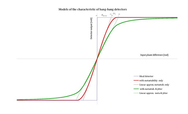
Finite gain of bang bang detectors: Metastability and phase noise[edit | edit source]
The two most relevant phenomena that alter the ideal model of the phase detector away from vertical slopes and infinite gain are the metastability of the detector flip-flops and the phase noise at its inputs.
- Metastability
The flip-flops that make up a bang-bang PD, when operated with very small input signal, are affected by metastability.
This becomes relevant when fp is so high that the metastable transient lasts for a significant part of the sampling period.[12]
Averaging across the clock cycle at constant input phase difference, the vertical slopes of the characteristic become less steep and the corners become rounded. A linear transition with finite slope is a simpler, still reasonably accurate, model.
- The ± π region is the only one under consideration now.
- Parts of the characteristic with negative slope, that are unstable in closed loop operation, are of no interest. In many practical cases, where PFDs are used, those slopes are even invisible, masked by the frequency detection mechanism.
The width of the region of linear transition is ±Φ, ±Φmeta in this case.
- Phase noise i.e. unwanted jitter
In design, characterisation and measurement, a sinusoidal jitter is used to explore the characteristics.
At the comparator input, this signal always has additional components originated primarily by ISI and VCO noise.
This additional phase noise can be modelled by including its effect in the model of the comparator.
The overall characteristic is further spread out, and this corresponds to the convolution of the "intrinsic" characteristic with the noise probability density function.[13]
- It is like a low pass filtering of the comparator intrinsic characteristic.
The overall effect is reasonably well modelled again by a linear slope, where the transition region widens to Φmeta + 2σ, with σ being the standard deviation of the phase noise.[13]
All curves at DT = 1.
The average detector gain (output volts divided by input radians) loses its very high peak, and becomes correspondingly more realistic.
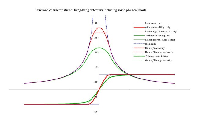
All curves at DT = 1.
.
External References[edit | edit source]
- ↑ a b c d Richard C. Walker (2003). "Designing Bang-Bang PLLs for Clock and Data Recovery in Serial Data Transmission Systems" (PDF). pp. 34-45, a chapter appearing in "Phase-Locking in High-Performance Systems - From Devices to Architectures", edited by Behzad Razavi, IEEE Press, 2003, ISBN 0-471-44727-7.
- ↑ A Monolithic 156 Mbit/s Clock and Data Recovery PLL Circuit Using the Sample -and-Hold Technique by Noboru Ishihara and Yukio Akazawa, IEEE Journal of Solid-State Circuits, vol. SC-29, pp. 1566-1571, December 1994
- ↑ A 2.5 Gbit/s Clock and Data Recovery IC with tuneable Jitter Characteristics for Use in LAN's and WAN's by Keiji Kishine, Noburu Ishihara, Ken-ichi Takiguchi, Haruhiko Ichino, 1999, a paper inserted in : Phae-Locking in High-Performance Systems, edited by Behzad Razavi 2003
- ↑ Hogge, C., “A Self Correcting Clock Recovery Circuit,”. IEEE TRANSACTIONS ON ELECTRON DEVICES, VOL. ED-32, NO. 12, DECEMBER 1985, pp. 2704-2706.
- ↑ a b J.D.H. Alexander, "Clock Recovery from Random Binary Signals", vol. 11, pp. 541 - 542, October 1975 in Electronics Letters. © Institution of Electrical Engineers.
- ↑ Jafar Savoj and Behzad Razavi, A 10-Gb/s CMOS Clock and Data Recovery Circuit with a Half-Rate Linear Phase Detector, IEEE JOURNAL OF SOLID-STATE CIRCUITS, VOL. 36, NO. 5, MAY 2001, http://www.seas.ucla.edu/brweb/papers/Journals/S&RMay01.pdf
- ↑ Floyd M. Gardner, "Charge-Pump Phase-Lock Loops", vol. COM-28, NO.11, pp. 1849 - 1858, November 1980 in IEEE TRANSACTION ON COMMUNICATION.
- ↑ Jri Lee; et al. "Modeling of Jitter in Bang-Bang Clock and Data Recovery Circuits" (PDF). II. BANG-BANG PD MODEL. Retrieved 2015-2-3.
{{cite web}}: Check date values in:|accessdate=(help); Explicit use of et al. in:|author=(help) - ↑ Jri Lee, Member, IEEE, Kenneth S. Kundert, and Behzad Razavi, Fellow, IEE (SEPTEMBER 2004). "Analysis and Modeling of Bang-Bang Clock and Data Recovery Circuits". IEEE JOURNAL OF SOLID-STATE CIRCUITS, VOL. 39, NO. 9, SEPTEMBER 2004 pages 1571 .. 1580. Retrieved 2015-2-3.
{{cite web}}: Check date values in:|accessdate=and|date=(help)CS1 maint: multiple names: authors list (link) - ↑ FLOYD M. GARDNER. "Charge-Pump Phase-Lock Loops". IEEEE TRANSACTIONS ON COMMUNICATIONS,VOL. COM-28, NO. 11, NOVEMBER 1980 pages 1849 .. 1858. Retrieved 2015-2-3.
{{cite web}}: Check date values in:|accessdate=(help) - ↑ FLOYD M. GARDNER (OCTOBER 1982). "Phase Accuracy of Charge Pump PLL's" (PDF). IEEE TRANSACTIONS ON COMMUNICATIONS, VOL.COM-30, NO. 10, OCTOBER 1982 pages 2362 .. 2363. Retrieved 2015-2-3.
{{cite web}}: Check date values in:|accessdate=and|date=(help) - ↑ Jri Lee, Kenneth S. Kundert, Behzad Razavi (SEPTEMBER 2004). "Analysis and Modeling of Bang-Bang Clock and Data Recovery Circuits". IEEE JOURNAL OF SOLID-STATE CIRCUITS, VOL. 39, NO. 9 pages 1571 .. 1579, II. BANG-BANG PD MODEL, A. Effect of Metastability. Retrieved 2015-1-25.
{{cite web}}: Check date values in:|accessdate=and|date=(help); Italic or bold markup not allowed in:|publisher=(help)CS1 maint: multiple names: authors list (link) - ↑ a b Jri Lee, Kenneth S. Kundert, Behzad Razavi (SEPTEMBER 2004). "Analysis and Modeling of Bang-Bang Clock and Data Recovery Circuits". IEEE JOURNAL OF SOLID-STATE CIRCUITS, VOL. 39, NO. 9 pages 1571 .. 1579, II. BANG-BANG PD MODEL, B. Effect of Jitter. Retrieved 2015-1-25.
{{cite web}}: Check date values in:|accessdate=and|date=(help); Italic or bold markup not allowed in:|publisher=(help)CS1 maint: multiple names: authors list (link)