Clock and Data Recovery/Structures and types of CDRs/The CDR' VCO
The VCO is a fundamental piece of every slave CDR.
VCO characteristic[edit | edit source]
A VCO block is present in some (not all) types of CDRs.
The VCO (Voltage Controlled Oscillator) is a circuit that outputs a single frequency signal (some VCOs output a sinusoid, some VCOs output a squarewave) in response to the level of the signal applied to its input; the frequency of its output is proportional to the value of its input signal (the latter is sometimes an analog voltage, sometimes a digital number):
It is convenient to study the PLL in the s or jω domain using the phase as the output variable. The model equation is then:

- The VCO shall be made track the frequency of the incoming signal pulses (fp) by the closed loop operation of the PLL.
As the free-running frequency characteristic of the VCO, ffr, never exactly coincides with fp, the control signal -while the PLL is tracking the input signal - exhibits an offset from its center value, proportional to the frequency mismatch:
where:
Ed should not be confused with Es (that has been introduced earlier in this book and that will be addressed again in some special cases again further on).
The VCO is very often the most critical block in the CDR, because
- it operates at the frequency of the received line pulses fp (or close to). It uses therefore the fastest circuitry in the PLL, along with the phase comparator.
- the value of ffr must be very precise. Precise component like quartz crystals or trimmed R, C, L must therefore be used inside the VCO (The phase comparator does not require precise components).
- it generates most of the added phase noise that the PLL cannot reject or mitigate.
The block that precedes the VCO, and that drives it, i.e. the amplifier/filter, is less critical in the sense of cost, need of precise components and noise.
As a consequence, it is convenient and correct to model and to simulate the PLL under the simplifying hypothesis that the circuit that drives the VCO matches exactly with its output range the input range of the VCO connected to it.
Frequency accuracy[1] of the VCO[edit | edit source]
The free-running frequency of the VCO ffr represents what the CDR knows about the frequency (fp) of the signal to lock into.
The difference (fp – ffr) is a known parameter of the CDR, called accuracy and often expressed in ppm as: (fp – ffr) / fp .
- When the acquisition begins, the fp – ffr accuracy is also the maximum drift in a second (in cycles per second = Hz, or in rad/esc) between the phase of the signal to lock into and the phase of the free-running VCO.
The knowledge about the variability of fp with time is embodied in a parameter of the overall PLL: its bandwidth.
- All PLLs have a low pass behaviour with respect to the processing of the input phase signal, and their cut-off frequency is called:
- fC [Hz] by the ITU-T that mostly refers to the equipment behaviour at its external interfaces,
- ωn or ωn2 [rad/s] when using linear models,
- ω-3 dB in some technical papers.
The CDR must track, first of all, any possible out of tune between fp and the VCO free running frequency ffr.
- This is the same as stating that frequency acquisition precedes phase acquisition.
The difference fp - ffr may be negligible in certain cases (and the frequency acquisition be hidden in the first part of the phase acquisition), but often it is not.
fp - ffr relevance[edit | edit source]
- Cost
The VCO types have largely different costs, and fp – ffr accuracies. The VCO choice may lead to different CDR architectures:
- high cost, i.e tight accuracy, ( fp – ffr) / fp < 100 ppm.
This is normally associated with high VCO gain and with low VCO noise (= e.g. quartz oscillators).
The PLL cut off frequency can be larger than the accuracy (=incoming frequency uncertainty), leading to slip-less acquisition and no need of a PFD.
- low cost, i.e poor accuracy, ( fp – ffr) / fp >> 100 ppm.
The VCO gain is normally lower, and the VCO noise larger (e.g. = LC and ring monolithic).
If the cut-off frequency must be close to or tighter than the accuracy, a PFD is required.
- dc performances
- The fp-ffr difference always always causes a steady state offset in the PLL node between the filter and the VCO ( a steady state drive error Ed).
- In the PLLs of type 1 - fp-ffr causes also a non-zero steady state offset between the inputs to the phase comparator (a sampling error Es ) .
- ac performances
- The difference fp - ffr (in association with the comparator type, the PLL gain and the possible slew-rates) is fundamental for the definition of the acquisition time and of the PLL bandwidth.
- When the difference fp-ffr is so large that it is comparable with, or that it exceeds the bandwidth of the CDR, the use of a PFD is mandatory. The frequency acquisition, in such cases, is often associated with slips and may last longer than the phase acquisition that follows.
- Frequency accuracy and PLL acquisition time
- The (in)accuracy unbalances the VCO, increasing the variation possible for the frequency in one direction at the expenses of variation possible in the other direction.
- In the direction towards higher frequencies , the VCO phase catch up with fp faster than fup = fmax - ffr,
in the direction towards decreasing frequencies the VCO can not let fp catch up with itself faster than fdown = ffr - fmin. - fmax and fmin are in some conditions forced very much closer to ffr than the extremes of the control range of the VCO.
- Typical is case of the 2nd order type 2 CDR in tracking condition, where the high frequency attenuation of the loop filter limits substantially the swing of the VCO drive signal.
- The PLL VCO is normally kept in its free running state as long as an incoming signal is not detected (LOS = Loss Of Signal condition).
- When released to hunt for the phase lock (i.e. when the LOS is de-asserted), the PLL acquisition transient does not differ from its normal reaction to an abrupt input step variation.
The magnitude of the step is the (random) phase and frequency difference between the VCO output and the input signal that just popped up.- 1. If the VCO accuracy is smaller (= tighter) than both fup and fdown
- in the cases where linear models can be used, the acquisition time is about 1/ωn for a first order PLL, and of about 2/ωn2 for a second order PLL. (Time needed to recuperate about 70% of the distance from the optimum lock-in condition independently of the magnitude of the step).
- If the VCO is driven directly by a bang-bang detector, the VCO is driven by a signal that remains at either its highest or at its lowest value. The output phase of the VCO follows a linear ramp with a slope equal to Drive_voltage/GVCO all during the acquisition.
- 2. If the VCO accuracy is wider (= poorer) than either fup or fdown
- A PFD is present, and the acquisition may take several clock drift cycles and may include slips, depending on the initial frequency and phase differences.
- 1. If the VCO accuracy is smaller (= tighter) than both fup and fdown
- Frequency accuracy and PLL tracking bandwidth
- 1. The VCO accuracy is a limit to how tight the dejittering bandwidth can be If the open loop gain is finite.
- Linear CDRs with type 1 feedback do need a finite, non-zero, error at the input to maintain the drive error that locks the VCO.
- The sampling error, necessary to maintain the VCO locked to the PLL input, is proportional to the VCO frequency accuracy and inversely proportional to the DC forward Gain.
- 1. The VCO accuracy is a limit to how tight the dejittering bandwidth can be If the open loop gain is finite.
- Frequency accuracy and PLL tracking bandwidth


- In type 1 loops the natural frequency and the open loop DC gain are tightly related.


- For an open loop dc gain and a filter time constant , the jitter cut-off frequency of a linear 2nd order type 1 loop is:


It is easy to see that, for a 1st order type 1 loop: Es = ((ωp – ωfr) / ωn1
- The same equation, rearranged, tells that the frequency mismatch and the maximum Es define how tight (relative to the line frequency) the loop jitter bandwidth can be:


It is easy to see that, for a 1st order type 1 loop: (ωn1/ωp ) = ((ωp – ωfr) /ωp) / Es )
- For the maximum allowed sampling error, there is a minimum jitter transfer (=dejittering) bandwidth.
- 2. If the open loop gain is very large (infinite), the VCO accuracy is not fundamental for the jitter transfer characteristic.
- The jitter transfer characteristic varies with the input jitter amplitude, and is a consequence of slewing as the VCO control signal saturates at the ends of its range.[2]
Relative concept[edit | edit source]
Jitter as well as frequency accuracy are both relative concepts.
They describe the relative mismatch of two quantities (two phases that are functions of time, or two frequencies). The mismatch does not need:
- either of the quantities to be considered the reference for the other;
- a third quantity as independent reference.
- One of the two quantities is in general expected to jitter less of the other with respect to a third reference clock like the Primary Reference Clock in a telecommunication network, or the clock reference of the best measurement instrument available in the test set-up.
- With respect to the (much more accurate) master clock, the free running frequency of a slave CDR may differ no more than 50 ppm from the frequency of its remote master (very low cost quartz crystal), or 5000 ppm (monolithic RC oscillator after EWS trimming), or even differ less than 1 ppm, still without big cost concerns (quartz for GPS receivers inside mobile phones). Less than 0.1 ppm is typical of professional equipment.
The VCO of the PLL is a frequency modulator[edit | edit source]
- The stand alone VCO block is a frequency modulator by definition
- The VCO of a CDR (see also its description at the beginning of this page) performs in full compliance with the definition of frequency modulation.
- In normal tracking, the VCO modulation is a narrowband FM (h < 0.3).
The whole PLL seen as a frequency de-modulator[edit | edit source]
When a VCO is part of a PLL, the VCO output coincides with the PLL output.
The VCO input instead is a node whose signal tells exactly the frequency at which the VCO, and therefore the PLL, shall operate.
Such frequency is : .

In the following pages, the overall PLL transfer function (from the phase of the PLL input to the phase of the PLL (=of the VCO) output ) will be obtained for different PLLs, combining the individual transfer functions of phase comparator, amplifier/filter and VCOs.


Such overall transfer function is called the PLL “jitter transfer function”:

The VCO transfer function, when the phase is the output variable, is .

The transfer function of the PLL, from input phase to VCO input is:

If, instead of the PLL input phase , the PLL input frequency is considered, must be replaced by its derivative, because the frequency is the derivative of the phase. The derivative of , i.e. is: . The frequency demodulation transfer function is therefore:


Apart from the fixed coefficient , the frequency "demodulator" transfer function (PLL input frequency to VCO input voltage representing a frequency) is the same as the PLL phase jitter transfer function (PLL input phase to PLL output phase (= VCO output phase)) !

In other words, the PLL can be seen as a frequency demodulator of the signal at its input where the VCO input acts as the frequency demodulator output!
This conclusion may help later in the book to quicker visualize the PLL behavior in some special cases and conditions.
For instance, all PLLs have phase (=jitter) transfer functions with 0 dB gain from 0 to the frequency cut-off where the jitter low-pass starts.
The very same frequency diagram (just scaled by the value ) holds good for the inherent frequency demodulator, with the same bandwidth, etc.
Modeling and simulation of the VCO[edit | edit source]
- with (in)accuracy included

Both in the model equations and in the simulation calculation formulae,
the finite accuracy of the VCO can be taken into account adding an input bias to the (ideal) VCO.
VCO model[edit | edit source]

The VCO function is represented as a block with linear relation of its input signal (ranging around 0 volt) with respect to its output frequency (that ranges correspondingly around ffr).
It is more convenient to consider the instantaneous phase of the VCO output as output variable, because the inclusion of a VCO block in a PLL model becomes straightforward.
Phase and frequency are related by a differential operation, as the phase is the integral function of the frequency and the latter is the derivative of the former.
As angular frequencies in preference to period frequencies are used in conjunction with Laplace transforms (s = r +jω), the VCO gain GVCO is expressed in [rad/sec/volt] and the (precisely centered) VCO transfer function is written as (see the figure above):
The drive error Ed, preceded by a minus sign, is the signal addition needed at the VCO input to take into account in the model the lack of accuracy of the VCO itself.
A VCO that is absolutely accurate becomes “inaccurate” by the amount (ωp - ωfr) if a d.c. bias equal to -Ed is added at its input.
The saturation outside the range ωmin...ωmax is not taken into account by the model, that is linear. Such non-linearity is incorporated instead in the simulation equations.
VCO simulation[edit | edit source]
If the input signal reaches outside +/- 1 volt (see the purple "Curve for simulation" in the figure above), the (simulated) VCO freezes itself either at ωmin or at ωmax, depending whether the input signal is lower than -1 or greater than +1.
To take into account the VCO accuracy (i.e. the mismatch between ωp and ωfr), the VCO shall be simulated as:
The amplifier/filter output swings between -1 and 1 volt, with 0 volt corresponding to 0 volt at its input.
Clamping completes the computation of the amplifier output signal,
simulating at the same time both the amplifier/filter output limitation and the VCO range limitation.
After clamping this output to +/-1 volt, the -Ed bias is added.
As a result, the simulated VCO runs at ωfr when the filter output is 0 volt, ωmax when the filter output is +1 volt and ωmin when the filter output is -1 volt.
To simulate the conversion of the output frequency (linearly proportional to the VCO input) into the output phase, an integration is made.
The first value is computed as the first VCO input multiplied by the discrete time step of the simulation.
Any subsequent entry is the previous value incremented by the present VCO input multiplied by the discrete time step of the simulation.
To take into account the VCO gain, the result obtained in the previous calculation is multiplied by GVCO and the simulated value of the VCO output is obtained.
The PLL closed loop simulation, in addition to the Ed value, will also show the transient and the final value of the corresponding steady state error Es (if finite).
Different types of VCOs[edit | edit source]

The Sections above have presented with some detail the classic VCO model (that is a valid model for many VCOs in actual CDRs) and have given suggestions on how to simulate it.
The ring oscillator is an example.
It is often used in monolythic CDRs[3] where VCO low noise is not the prime requirement. (An LC oscillator -hybrid or monolythic- is used used in that case[4]).

Depending on the signal processing element in the loop (a flat amplifier or an integrator),
the DLL loop can be of 0th order and type 0 or of 1st order and type 1.
When analyzing existing CDRs, different VCOs may be encountered, and a different simulation or model may be more appropriate:
- bang-bang between two frequencies [5](simple although somewhat noisy, can be integrated easily inside an IC).
- Fixed free running frequency ffr, followed by a variable ratio divider...(possible if the technology allows a start frequency much higher than ωp). The inherent non linearities of the characteristic can be made smaller if a higher start frequency can be chosen and if the division ratio can be controlled with many close steps.
- A DLL whose output can be sequentially (and circularly) taken from the output of each of its stages by a multiplexer, so that the output phase can be varied indefinitely. The multiplexer could be driven:
- by a A/D conversion of the control signal. The resulting VCO is an oscillator controlled in phase and its model is simply a fixed gain. The gain is equal to the delay line control gain Gdl multiplied by the A/D gain (sec/volt) if the VCO output is measured in seconds, or equal to to Gdl x GA/D multiplied by the ratio: delay_line_length / oscillator_angular_frequency, if the VCO output is measured in radian.
- by an integrator plus A/D ( or by an accumulator if the implementation is digital) and then to the control input of the delay line. This adds a 1/s factor to the VCO model
VCO noise[edit | edit source]
No oscillator is exempt from noise, and the oscillator noise affects the CDR performances.
The output waveform of an oscillator is never perfect in shape and immobile at its nominal frequency. Its power is not an impulse at ffr, but it is distributed around it and exhibits a sort of "bell" shape.
Noise may in theory affect the amplitude, or the phase, or both, in the waveform produced by the oscillator.[6]
Avoiding non-fundamental discussions, it is always assumed that the amplitude of the output waveform of an oscillator is constant and does not contribute to the oscillator noise.
Just its phase (phase or frequency, which is the same thing) jitters and generates the noisy behavior.
In other words, the oscillator noise that can be measured is made up of phase noise only.[7] This assumption corresponds to the condition that there is no correlation between the power in the upper and lower side-bands.[6]
It is also generally assumed that phase noise is small and can be treated with linear models. This assumption practically corresponds to the condition that the total jitter corresponding to the phenomena under investigation never exceeds π/10.[6]
When a CDR is left free-running because no received signal is present (LOS Loss Of Signal = 1), then all the VCO phase noise is present at the CDR otput. (This is relevant and may become problematic in regenerators, but is not very relevant in end-points and in phase-aligners).
When the CDR is regularly operating and locked, the VCO frequency shifts and coincides with fp.
It will be shown that, when the CDR is in lock, the VCO phase noise that reaches the CDR output is progressively attenuated from the loop characteristic frequency downwards.
Very close to fp the VCO phase noise that reached the CDR output is attenuated to negligible levels.
How much an oscillator deviates from the ideal behavior is normally described by its Power Spectral Density, PSD.
The PSD is always finite, and peaks at ffr when the oscillator (the VCO) is free-running, or at fp when the VCO is locked.
When a CDR is in lock, the PSD of the VCO, centered around fp, exhibits essentially the same side-bands than when free-running.
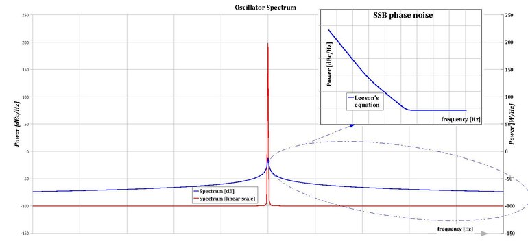
The PSD curve looks different if the vertical axis scale is logarithmic (used when the side-bands are important) or if the scale is linear (used when the fundamental frequency of oscillation is more important than the side-bands)
The Power Spectral Density of an oscillator can be measured in dBc/Hz (or in another logarithmic unit, that yields the same curve but translated upwards or downwards) or in W/Hz (linear y-scale).
The horizontal x-axis is linear and centered on the fundamental frequency when PSD is described on both sides of ffr, to avoid asymmetrical representation of the two side-bands.
The phase noise proper L(f) (pronounced “script-ell of f”), is defined (and measured) as one half (= the upper half) of the double-sideband PSD of the oscillator. It is a function of the frequency offset between the frequency of measure and the oscillator center frequency.
It may be noted that the definition does not exactly include the oscillator center frequency (or frequency = 0 of phase noise). Very slow phase noise or wander is at the same time difficult to deal with and of difficult measure. It belongs to a different engineering topic, like a very little frequency offset or like a very selective spectrum analyzer or like a measurement that takes a very long time. As it is of very little or of no practical use for the engineering of phase noise in oscillators, it is left out.
When expressed in decibels, the units of L(f) are dBc/Hz (dB below the carrier in a 1 Hz bandwidth at a distance f from the center frequency).
Logarithmic axes[edit | edit source]
The logarithmic y-axis representation is necessary when the oscillator noise is measured.
If only the upper side-band of the oscillator phase noise is described, then also the x-axis is preferably logarithmic.
Modeling[edit | edit source]
Modeling of the oscillator noise describes just the upper side-band of the oscillator spectrum (and the preferred scale of the x-axis is also logarithmic).
In most practical cases, the oscillator noise PSD uses the oscillator fundamental frequency as a zero reference, and the difference f-ffr as independent variable.
To avoid unnecessary troubles (mathematical ∞/0 for a model; infinite selectivity and/or dynamic range for a measure), the description does not reach down to zero frequency difference, but gets very close (so that only a minor amount of power, i.e. PSD x frequency interval, is neglected).
The well known model was proposed by Leeson (February 1966).
A fundamental paper is also the one from A. Hajimiri and Thomas H. Lee (1998)[8]
External References[edit | edit source]
- ↑ ITU-T G.810 (08/96) - DEFINITIONS AND TERMINOLOGY FOR SYNCHRONISATION NETWORKS - page 5 - 4.5.3: " frequency accuracy: The maximum magnitude of the fractional frequency deviation for a specified time period. NOTE – The frequency accuracy includes the initial frequency offset and any ageing and environmental effect. "
- ↑ Analysis and Modeling of Bang-Bang Clock and Data Recovery Circuits, Jri Lee, Kenneth S. Kundert, and Behzad Razavi, IEEE JOURNAL OF SOLID-STATE CIRCUITS, VOL. 39, NO. 9, SEPTEMBER 2004, pages 1571..1580, III. JITTER ANALYSIS A. Jitter Transfer
- ↑ Analysis of Timing Jitter in CMOS Ring Oscillators, Todd C. Weigandt, Beomsup Kim and Paul R. Gray, Proc. of ISCAS, June 1994, a paper included in Monolithic Phase-locked Loops and Clock Recovery Circuits, Theory and Design, IEEE PRESS, ISBN 0-7803-1149-3
- ↑ Analysis, Modeling and Simulation of Phase Noise in Monolithic Voltage-Controlled Oscillators, Behzad Razavi in Proc. CICC, pp. 323-326, May 1995, a paper included in Monolithic Phase-locked Loops and Clock Recovery Circuits, Theory and Design, IEEE PRESS, ISBN 0-7803-1149-3
- ↑ Richard C. Walker (2003). "Designing Bang-Bang PLLs for Clock and Data Recovery in Serial Data Transmission Systems". pp. 34-45, a chapter appearing in "Phase-Locking in High-Performance Systems - From Devices to Architectures", edited by Behzad Razavi, IEEE Press, 2003, ISBN 0-471-44727-7.
- ↑ a b c IEEE Std 1139-1999 IEEE Standard Definitions of Physical Quantities for Fundamental Frequency and Time Metrology—Random Instabilities, http://www.umbc.edu/photonics/Menyuk/Phase-Noise/Vig_IEEE_Standard_1139-1999%20.pdf
- ↑ Clock (CLK) Jitter and Phase Noise Conversion, MAXIM APPLICATION NOTE 3359, http://www.maxim-ic.com/app-notes/index.mvp/id/3359
- ↑ A General Theory of Phase Noise in Electrical Oscillators, by Ali Hajimiri and Thomas H. Lee, IEEE JOURNAL OF SOLID-STATE CIRCUITS, VOL. 33, NO. 2, FEBRUARY 1998 http://www.chic.caltech.edu/Publications/general_full.PDF